Silicon carbide semiconductor device and method for manufacturing same

a silicon carbide semiconductor and semiconductor technology, applied in the direction of semiconductor devices, basic electric elements, electrical appliances, etc., can solve the problems of difficult to improve the dielectric breakdown resistance of the silicon carbide semiconductor device, the thickness of the thermal oxidation film is more difficult to form by thermally oxidizing the silicon carbide substrate, and the temperature and time are required. to achieve the effect of improving the dielectric breakdown resistan

Active Publication Date: 2015-08-20
SUMITOMO ELECTRIC IND LTD
View PDF12 Cites 5 Cited by
  • Summary
  • Abstract
  • Description
  • Claims
  • Application Information

AI Technical Summary

Benefits of technology

[0009]The present invention has been made to solve the foregoing problem, and has an object to provide a silicon carbide semiconductor dev

Problems solved by technology

Moreover, in order to form a thick thermal oxidation film by thermally oxidizing the silicon carbide substrate, higher temperature and longer time are required than those in thermally oxidizing the silicon substrate.
Thus, it is more difficult to form a thick thermal oxidation film by thermally oxidizing the silicon carbide substrate, as compared wi

Method used


Image

  • Silicon carbide semiconductor device and method for manufacturing same
  • Silicon carbide semiconductor device and method for manufacturing same
  • Silicon carbide semiconductor device and method for manufacturing same

Examples


Embodiment Construction

[0042][Description of Embodiments of the Invention of the Present Application]

[0043]The following describes embodiments of the present invention with reference to figures. It should be noted that in the below-mentioned figures, the same or corresponding portions are given the same reference characters and are not described repeatedly. Regarding crystallographic indications in the present specification, an individual orientation is represented by [], a group orientation is represented by , and an individual plane is represented by ( ), and a group plane is represented {}. In addition, a negative crystallographic index is normally expressed by putting “−” (bar) above a numeral, but is expressed by putting the negative sign before the numeral in the present specification.

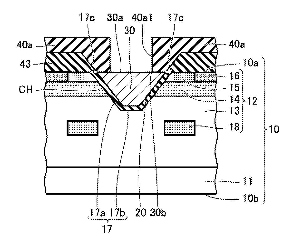
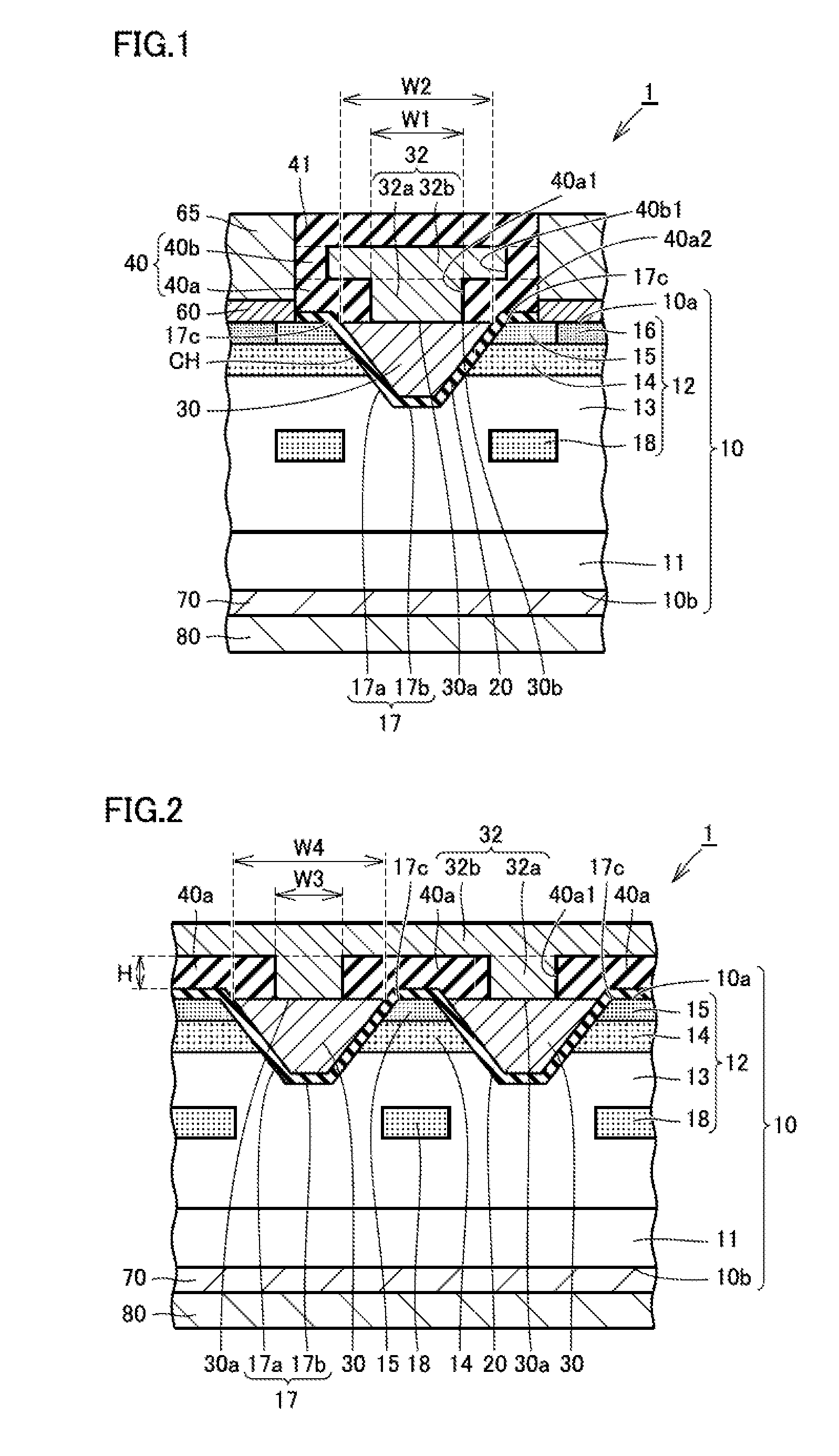
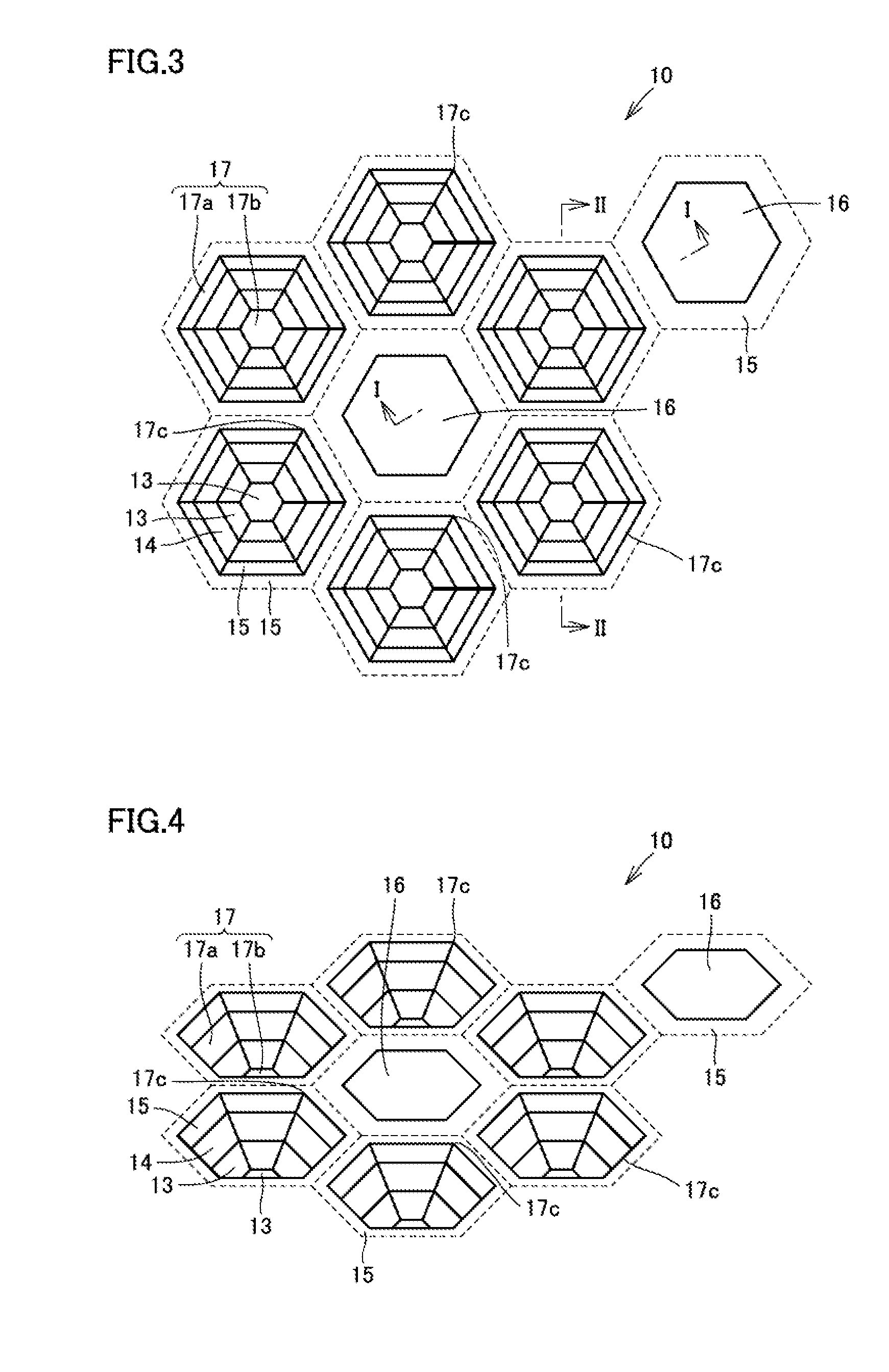
[0044](1) A silicon carbide semiconductor device 1 according to an embodiment includes a silicon carbide substrate 10, a gate insulating film 20, a gate electrode 30, an interlayer insulating film 40a, and a gate inter...


PUM


Abstract

A silicon carbide semiconductor device includes a silicon carbide substrate, a gate insulating film, a gate electrode, an interlayer insulating film, and a gate interconnection. The silicon carbide substrate includes: a first impurity region; a second impurity region provided on the first impurity region; and a third impurity region provided on the second impurity region so as to be separated from the first impurity region. A trench has a side portion and a bottom portion, the side portion extending to the first impurity region through the third impurity region and the second impurity region, the bottom portion being located in the first impurity region. When viewed in across section, the interlayer insulating film extends from above the third impurity region to above the gate electrode so as to cover the corner portion.

Description

BACKGROUND OF THE INVENTION[0001]1. Field of the Invention[0002]The present invention relates to a silicon carbide semiconductor device and a method for manufacturing the silicon carbide semiconductor device, in particular, a silicon carbide semiconductor device provided with a trench and a method for manufacturing such a silicon carbide semiconductor device.[0003]2. Description of the Background Art[0004]In recent years, in order to achieve high breakdown voltage, low loss, and utilization of semiconductor devices, such as a MOSFET (Metal Oxide Semiconductor Field Effect Transistor, under a high temperature environment, silicon carbide has begun to be adopted as a material for a semiconductor device. Silicon carbide is a wide band gap semiconductor having a band gap larger than that of silicon, which has been conventionally widely used as a material for semiconductor devices. Hence, by adopting silicon carbide as a material for a semiconductor device, the semiconductor device can h...

Claims


Application Information

Patent Timeline
IPC IPC(8): H01L29/78H01L29/66H01L21/02H01L29/423H01L29/04H01L29/16H01L29/49
CPCH01L29/7813H01L29/1608H01L29/66734H01L29/4916H01L21/02529H01L29/4975H01L29/4236H01L29/045H01L21/02271H01L29/495H01L21/02236H01L21/02247H01L21/02255H01L21/3065H01L29/42376H01L29/4941H01L29/66068H01L29/0623H01L21/046H01L21/0475H01L21/049
Inventor MASUDA, TAKEYOSHI
Owner SUMITOMO ELECTRIC IND LTD
Why Eureka
Try Eureka