

Nanoscale scanning sensors
- Summary
- Abstract
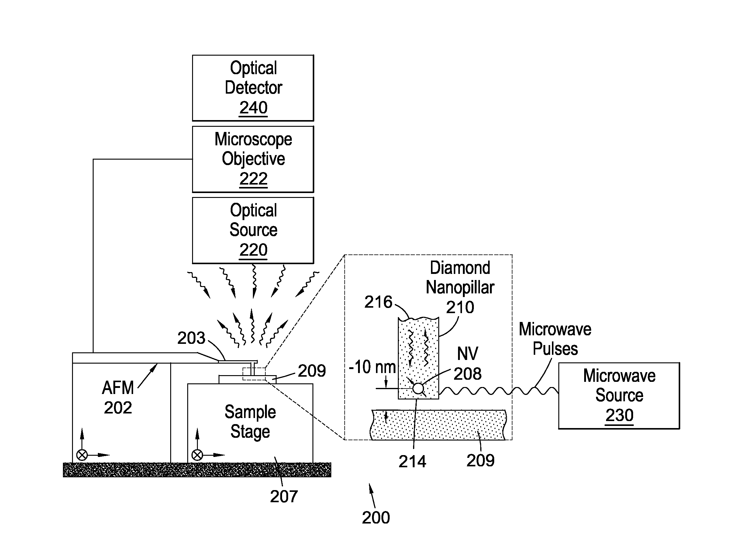
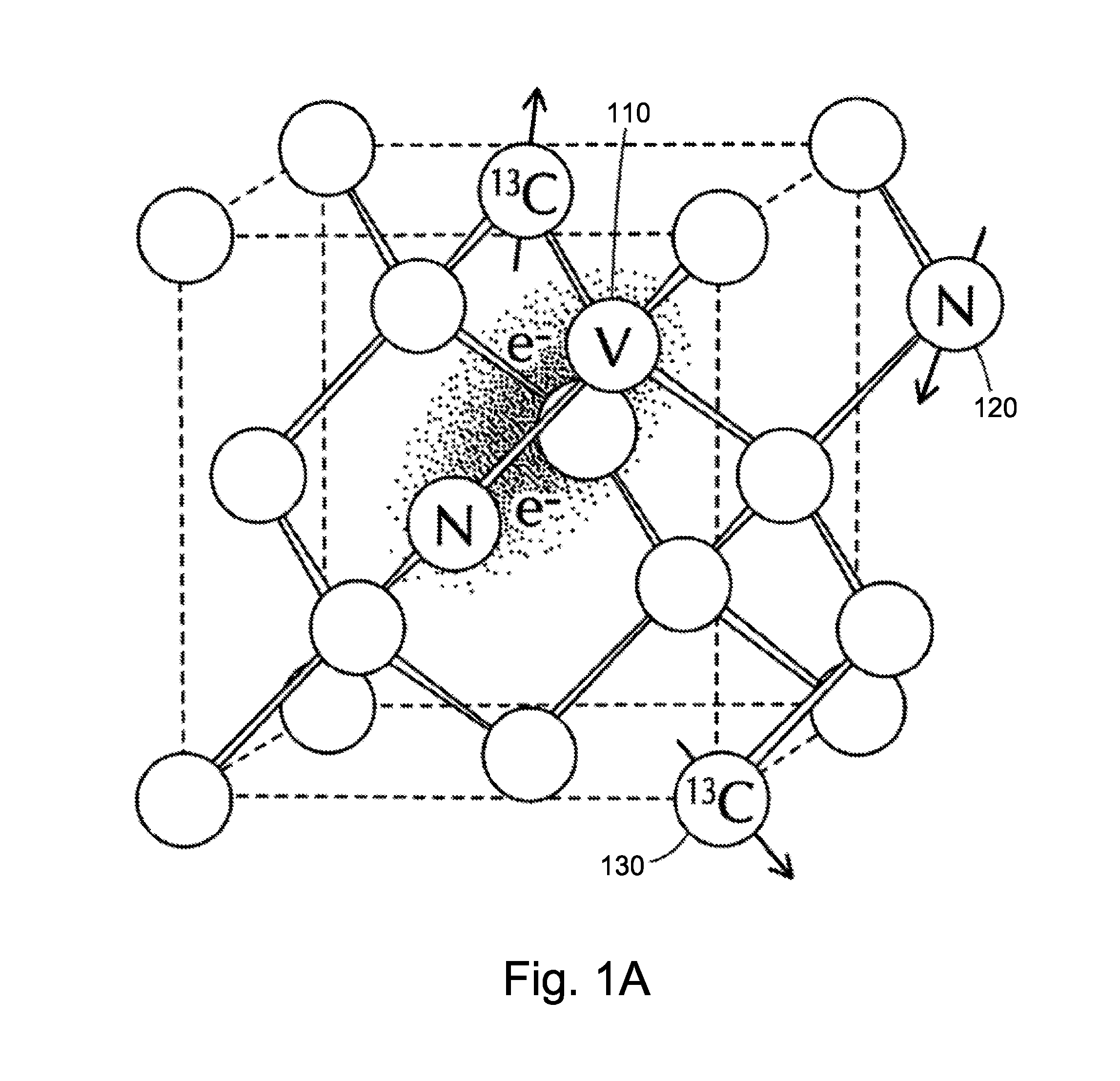
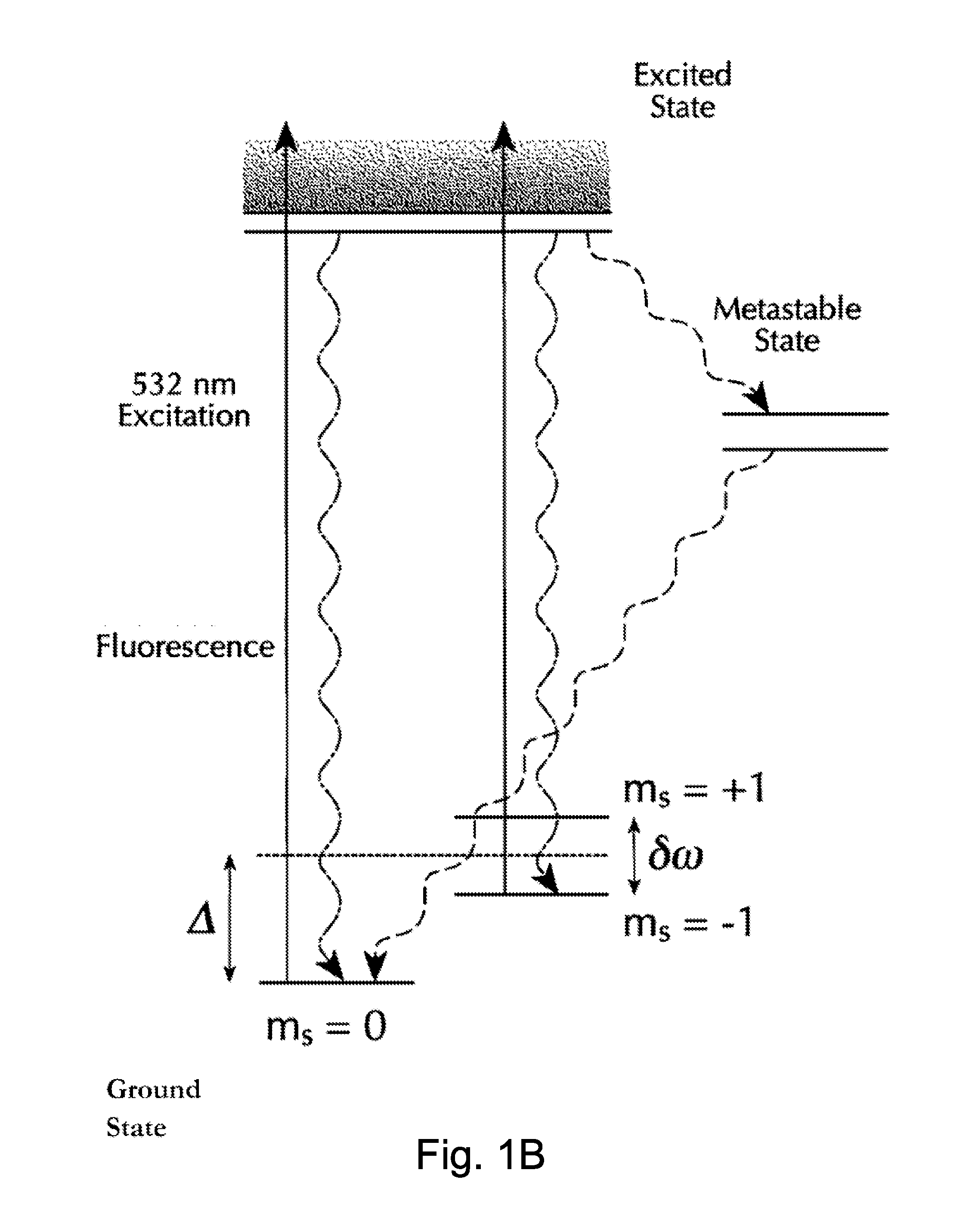
- Description
- Claims
- Application Information
AI Technical Summary
Benefits of technology
Problems solved by technology
Method used
Image

Examples
Embodiment Construction
[0064]Illustrative embodiments are discussed in this application. Other embodiments may be used in addition or instead.
[0065]It should be understood that the present application is not limited to the particular embodiments described, as such may vary. Also, the terminology used herein is for the purpose of describing particular embodiments only, and is not intended to be limiting, since the scope of the present application will be limited only by the appended claims.
[0066]Unless defined otherwise, all technical and scientific terms used herein have the same meaning as commonly understood by one of ordinary skill in the art to which this invention belongs. Although any methods and materials similar or equivalent to those described herein can also be used in the practice or testing of concepts described in the present application, a limited number of the exemplary methods and materials are described herein.
[0067]Where a range of values is provided, each intervening value, to the tenth...
PUM
 Abstract
Description
Claims
Application Information