Ultra-thin embedded semiconductor device package and method of manufacturing thereof

a technology of embedded semiconductors and packaging structures, which is applied in the direction of sustainable manufacturing/processing, printed circuit aspects, and final product manufacturing, etc., can solve the problems of dbc adding significant cost to the packaging structure, increasing the size of the module, and adding significant inductan

Active Publication Date: 2015-09-10
GENERAL ELECTRIC CO
View PDF14 Cites 143 Cited by
  • Summary
  • Abstract
  • Description
  • Claims
  • Application Information

AI Technical Summary

Benefits of technology

[0005]In accordance with one aspect of the invention, a package structure includes a first dielectric layer, at least one semiconductor device attached to the first dielectric layer, and an embedding material applied to the first dielectric layer so as to embed the at least one semiconductor device therein, the embedding material comprising one or more additional dielectric layers. The package structure also includes a plurality of vias formed in the first dielectric layer formed to the at least one semiconductor device, metal interconnects formed in the plurality of vias and on one or more outward facing surface of the package structure to form electrical interconnections to the at least one semiconductor device, and input / output (I / O) connections located on one end of the package structure on one or more outward facing surfaces thereof to provide a second level connection to an external circuit. The package structure is configured to interfit with a connector formed on the external circuit to mount the package perpendicular to the external circuit, with the I / O connections on the one end of the package structure being electrically connected to the connector to form the second level connection to the external circuit.
[0006]In accordance with another aspect of the invention, a method of manufacturing a semiconductor device package structure includes attaching at least one semiconductor device to a first dielectric layer by way of an adhesive, applying an embedding material on the first dielectric layer so as to be positioned about the at least one semiconductor device, and performing a lamination process to cause the embedding material to fill any air gaps present around the at least one semiconductor device and so as to embed the at least one semiconductor device therein, wherein the first dielectric layer does not melt or flow during the lamination process. The method also includes forming a plurality of vias to the at least one semiconductor device, forming metallic interconnects in the plurality of vias and over at least a portion of one or more outer surfaces of the package structure to form electrical interconnections to the at least one semiconductor device, and forming input / output (I / O) connections on one or more of the outward facing surfaces of the package structure, at only one end of the package structure, the I / O connections comprising electrical leads that provide a second level connection to an external circuit.
[0007]In accordance with yet another aspect of the invention, a package structure includes a first dielectric layer having an adhesive applied on at least a portion thereof, one or more semiconductor devices attached to the first dielectric layer by way of the adhesive, an embedding material positioned on the first dielectric layer about the one or more semiconductor devices so as to embed the one or more semiconductor devices therein, a plurality of vias formed to the at least one semiconductor device, metal interconnects formed in the plurality of vias to form all electrical and thermal interconnections to the one or more semiconductor devices and in the package structure and input / output (I / O) connections formed on at least one outer surface of the package structure to provide a second level connection to an external circuit, wherein the I / O connections are configured to interfit with a socket or recess formed in the external circuit, such that the package structure is partially embedded in the external circuit when the I / O connections of the package structure are interfit in socket or recess.

Problems solved by technology

Alternatively, especially for higher power ranges, the power modules packaging structures may have large terminals for connection to the external circuit which add significant inductance and increase the size of the module.
It is recognized, however, that the DBC adds significant cost to the packaging structure both from a materials standpoint and from a processing standpoint—as additional processing steps and temperature excursions are required when including a DBC in the packaging structure, such as soldering and flux cleaning processes required for joining the DBC to the packaging structure.
It is also recognized that the wirebonds and leads add significant parasitic inductance that reduces the efficiency of the package.
Wirebonds also add significant height to the package.
It is still further recognized that—while the leads on the packaging structure allow higher thermal cycling reliability and are not subject to stringent Moisture Sensitivity Level (MSL) Requirements—the leads or terminals in a power module can be quite large and affect the module foot-print and thickness on the PCB and also negatively impact the electrical performance due to high inductance.

Method used


Image

  • Ultra-thin embedded semiconductor device package and method of manufacturing thereof
  • Ultra-thin embedded semiconductor device package and method of manufacturing thereof
  • Ultra-thin embedded semiconductor device package and method of manufacturing thereof

Examples


Embodiment Construction

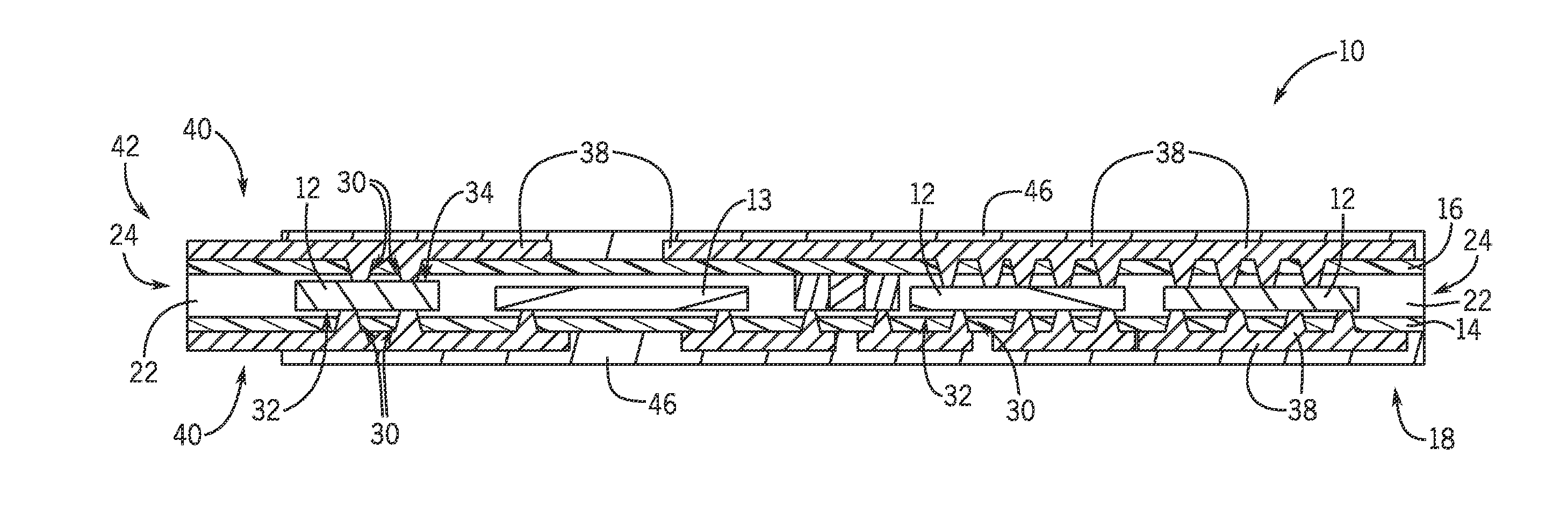
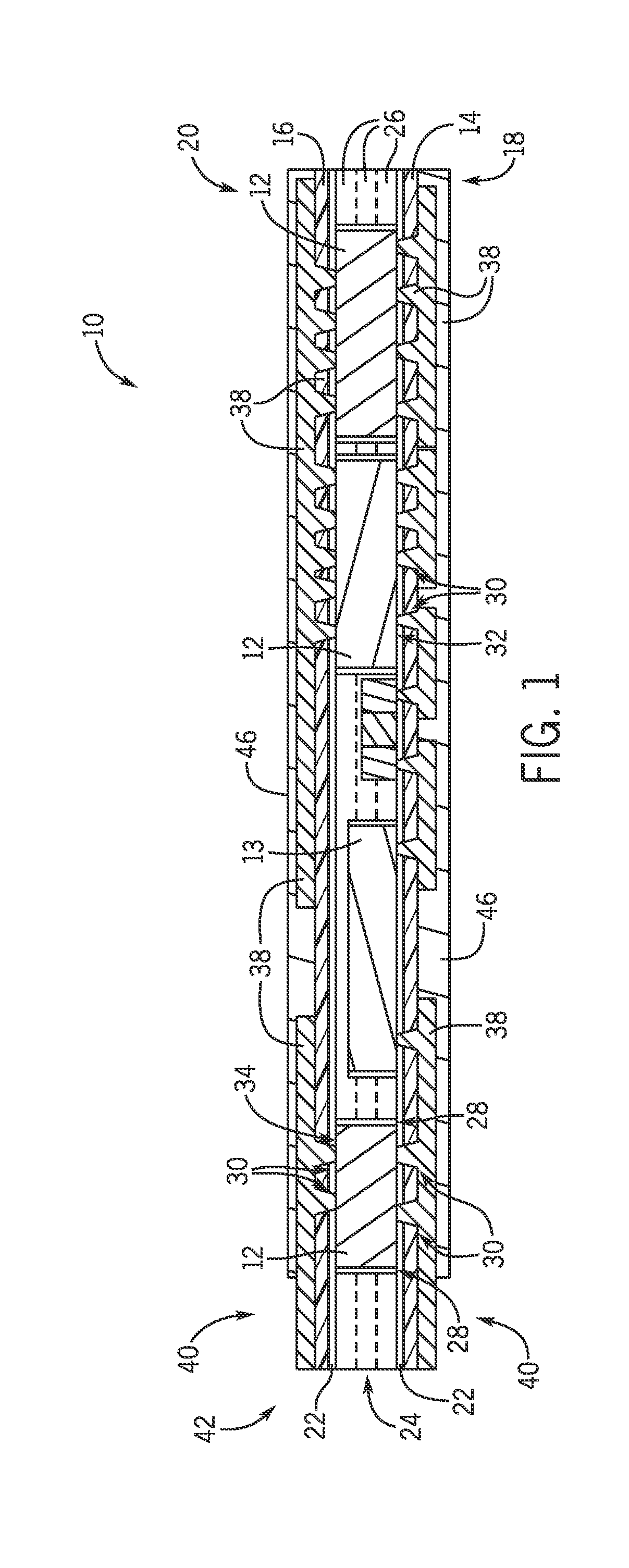
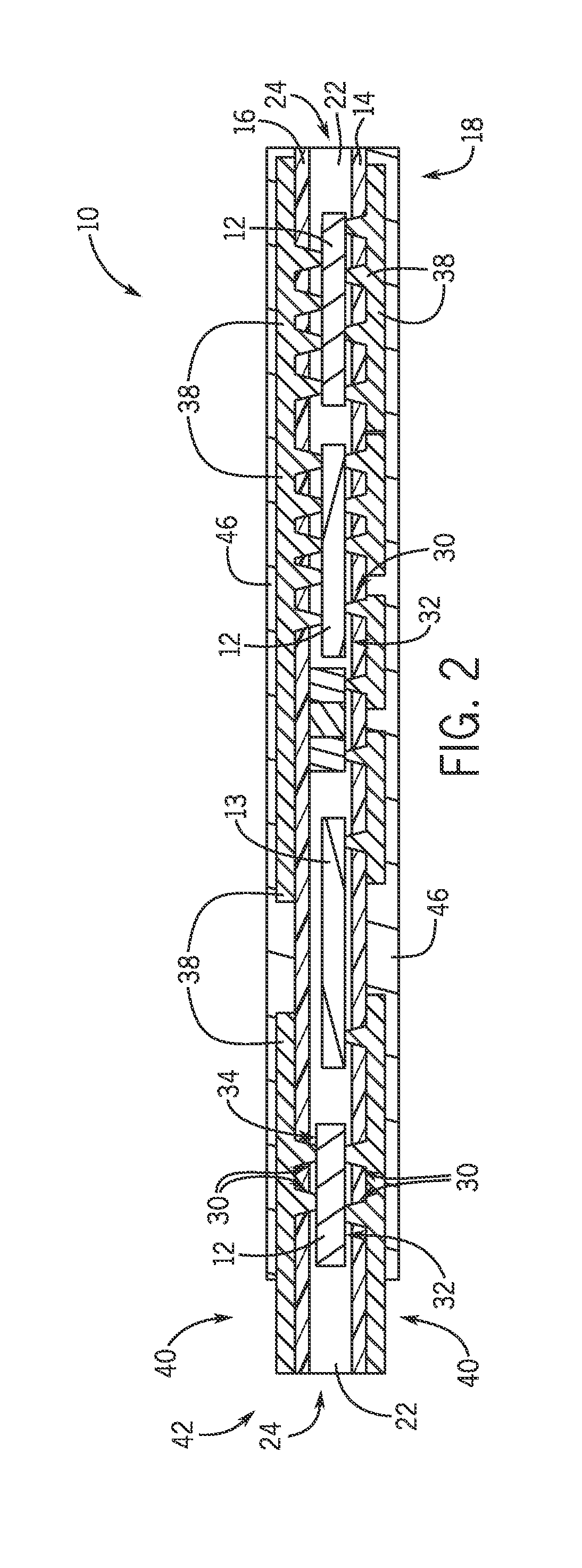
[0020]Embodiments of the present invention provide for an embedded power module package structure having power overlay (POL) interconnects that form all electrical and thermal interconnections to the semiconductor devices in the power module, as well as a method of forming such a package structure. The package structure is constructed to have an “ultra-thin” construction in two axes, and may be partially embedded in an external circuit (e.g., PCB) to which the package structure is mounted.

[0021]Referring to FIG. 1, a POL packaging and interconnect structure 10 is shown according to an embodiment of the invention. The package structure 10 includes one or more semiconductor devices 12, 13 that can be in the form of either what can generally be described as a “power device” or a “non-power device”, and thus can be in the form of a die, diode, MOSFET, transistor, application specific integrated circuit (ASIC), or processor, for example. While three power semiconductor devices 12 and a s...


PUM


Abstract

A package structure includes a first dielectric layer, semiconductor device(s) attached to the first dielectric layer, and an embedding material applied to the first dielectric layer so as to embed the semiconductor device therein, the embedding material comprising one or more additional dielectric layers. Vias are formed through the first dielectric layer to the at least one semiconductor device, with metal interconnects formed in the vias to form electrical interconnections to the semiconductor device. Input/output (I/O) connections are located on one end of the package structure on one or more outward facing surfaces thereof to provide a second level connection to an external circuit. The package structure interfits with a connector on the external circuit to mount the package perpendicular to the external circuit, with the I/O connections being electrically connected to the connector to form the second level connection to the external circuit.

Description

BACKGROUND OF THE INVENTION[0001]Embodiments of the invention relate generally to structures and methods for packaging semiconductor devices and, more particularly, to an ultra-thin power device packaging structure having power overlay (POL) interconnects that form all electrical and thermal interconnections in the structure, with the packaging structure having reduced inductance.[0002]Power semiconductor devices are semiconductor devices used as switches or rectifiers in power electronic circuits, such as switched mode power supplies, for example. In use, power semiconductor devices are typically surface mounted to an external circuit by way of a packaging structure, with the packaging structure providing an electrical connection to the external circuit and also providing a way to remove the heat generated by the devices and protect the devices from the external environment. Alternatively, especially for higher power ranges, the power modules packaging structures may have large ter...

Claims


Application Information

Patent Timeline
Patent Type & Authority Applications(United States)
IPC IPC(8): H01L23/00H01L23/367H01L23/373H01L25/10H01L23/48
CPCH01L24/32H01L2224/80365H01L23/481H01L23/373H01L23/367H01L24/46H01L24/43H01L24/27H01L24/83H01L2225/1094H01L2225/1052H01L2224/32501H01L2224/46H01L2224/43H01L2224/2711H01L25/105H01L23/34H01L23/42H01L23/433H01L23/5389H01L24/24H01L24/25H01L24/82H05K1/185H05K3/305H05K3/4602H01L2224/04105H01L2224/2402H01L2224/24137H01L2224/24195H01L2224/2518H01L2224/2919H01L2224/32225H01L2224/92144H01L2924/1033H01L2924/1203H01L2924/1304H01L2924/13091H01L2924/1433H05K1/0206H05K1/0209H05K1/183H05K3/301H05K3/306H05K3/366H05K2201/0195H05K2201/09845H05K2203/302H01L2224/05599H01L2224/85399H01L2924/00014H01L24/19H01L2224/45147H01L24/45Y02P70/50H01L2224/45015H01L2924/207H01L2224/43848
Inventor GOWDA, ARUN VIRUPAKSHAMCCONNELEE, PAUL ALANCHAUHAN, SHAKTI SINGH
Owner GENERAL ELECTRIC CO
Why Eureka
Try Eureka