Sensor device
- Summary
- Abstract
- Description
- Claims
- Application Information
AI Technical Summary
Benefits of technology
Problems solved by technology
Method used
Image

Examples
first embodiment
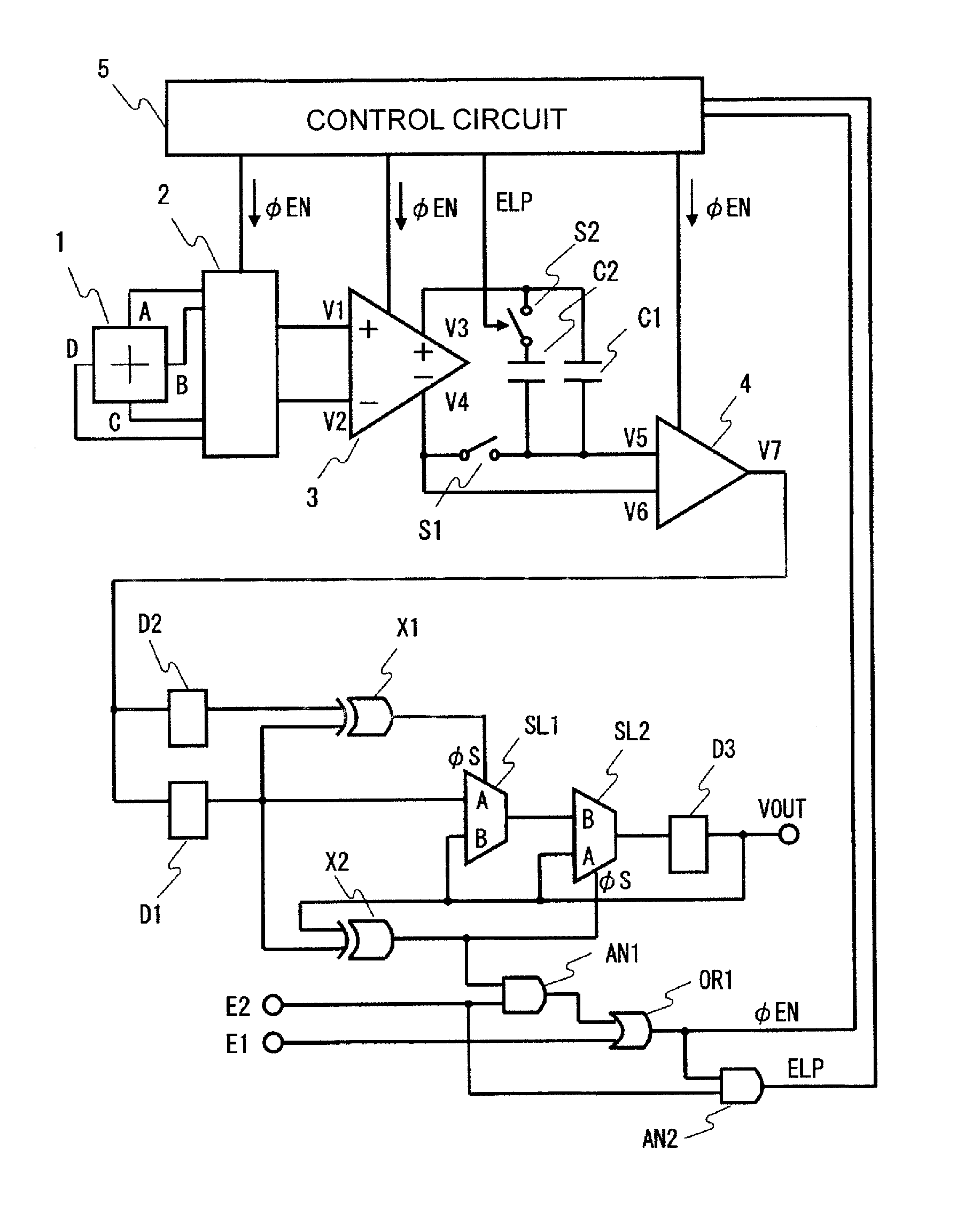
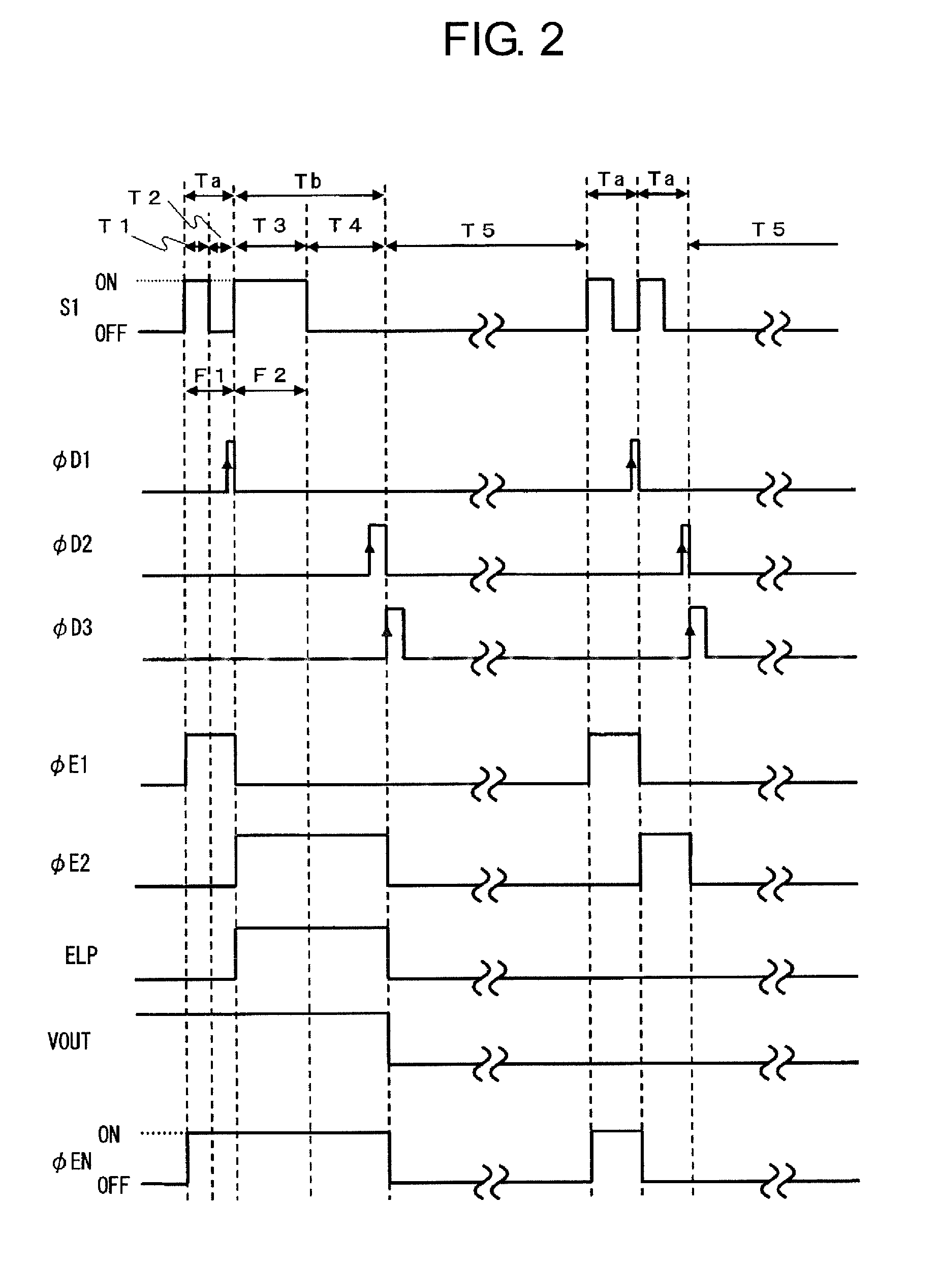
[0024]FIG. 1 is a circuit diagram illustrating a magnetic sensor device according to a first embodiment of the present invention. The magnetic sensor device of the first embodiment includes a Hall element 1 being the magnetoelectric conversion element, a switching circuit 2, a differential amplifier 3, a comparator 4, a control circuit 5, D type flip-flops D1, D2, and D3, XOR circuits X1 and X2, selector circuits SL1 and SL2, an AND circuit AN1, an OR circuit OR1, a capacitor C1 being an offset voltage storage capacitor, a capacitor C2 being an offset voltage storage and low pass filter capacitor, a switch S1, a switch S2, an output terminal VOUT, a terminal E1 for inputting an ON / OFF signal φE1, and a terminal E2 for inputting an ON / OFF signal φE2. The Hall element 1 has a first terminal pair A-C and a second terminal pair B-D. The switching circuit 2 has four input terminals respectively connected to the terminals A, B, C, and D of the Hall element 1, a first output terminal, and ...
second embodiment
[0042]FIG. 3 is a circuit diagram illustrating a magnetic sensor device according to a second embodiment of the present invention. The second embodiment differs from the first embodiment in that a low pass filter circuit L1 is arranged between the first output terminal of the differential amplifier 3 and the capacitor C1. FIG. 6 is a circuit diagram illustrating an example of the low pass filter circuit L1 used in the second embodiment. The low pass filter circuit L1 has an input terminal E11, an output terminal E13, a control terminal E15, a resistive element R21 arranged between the input terminal E11 and the output terminal E13, a switching circuit SW21 connected to the output terminal E13, and a capacitive element C21 arranged between the switching circuit SW21 and a ground. The switching circuit SW21 is controlled to be turned on and off based on a logic voltage input to the control terminal E15. When the switching circuit SW21 is turned on, the capacitive element C21 is connec...
third embodiment
[0043]FIG. 4 is a circuit diagram illustrating a magnetic sensor device according to a third embodiment of the present invention. The third embodiment differs from the first embodiment in that a capacitive element connected in parallel to a negative feedback resistor of a differential amplifier 103 is used for the low pass filter. FIG. 7 illustrates a configuration example of the differential amplifier 103 used in the third embodiment. The differential amplifier 103 has a positive input terminal E11, a negative input terminal E12, a positive output terminal E13, a negative output terminal E14, a control terminal E15, first and second operational amplifiers 11 and 12, first to third resistive elements R11 to R13, first and second capacitive elements C11 and C12, and first and second switching circuits SW11 and SW 12. A negative input terminal of the first operational amplifier 11 is connected to one terminal of the first resistive element R11, and an output terminal of the first oper...
PUM
 Abstract
Description
Claims
Application Information
 - R&D
- Intellectual Property
- Life Sciences
- Materials
- Tech Scout
- Unparalleled Data Quality
- Higher Quality Content
- 60% Fewer Hallucinations
Browse by: Latest US Patents, China's latest patents, Technical Efficacy Thesaurus, Application Domain, Technology Topic, Popular Technical Reports.
© 2025 PatSnap. All rights reserved.Legal|Privacy policy|Modern Slavery Act Transparency Statement|Sitemap|About US| Contact US: help@patsnap.com