Optical modulator and optical modulation device

a technology of optical modulator and optical modulator, which is applied in the direction of instruments, non-linear optics, optics, etc., can solve the problems of difficult to realize the optical phase difference between two arms having the same length, and the inability to achieve a highly integrated optical modulator, etc., to achieve high integration of optical modulators, low power consumption, and the effect of minimization in siz

Active Publication Date: 2015-10-01
NEC CORP
View PDF11 Cites 8 Cited by
  • Summary
  • Abstract
  • Description
  • Claims
  • Application Information

AI Technical Summary

Benefits of technology

[0025]According to the present invention, it is possible to achieve an optical modulator which can be miniaturized in size and which can operate with low power consumption. Additionally, it is possible to achieve an optical modulation device including high integration of optical modulators.

Problems solved by technology

Changes of refractive indexes in optical waveguides may cause changes of optical waveguide conductions, thus causing an optical phase difference between two arms having the same length.
For this reason, it is impossible to achieve a highly-integrated optical modulator.
This makes it difficult to realize a highly-integrated optical modulator.
This technology needs an optical phase modulation length on the order of millimeters, which makes it difficult to reduce the size of an optical modulator.
Since this technology inevitably increases the size of an optical modulator, it is impossible to achieve a highly-integrated optical modulator.

Method used


Image

  • Optical modulator and optical modulation device
  • Optical modulator and optical modulation device
  • Optical modulator and optical modulation device

Examples


Embodiment Construction

[0045]The present invention will be described in further detail by way of examples with reference to the accompanying drawings.

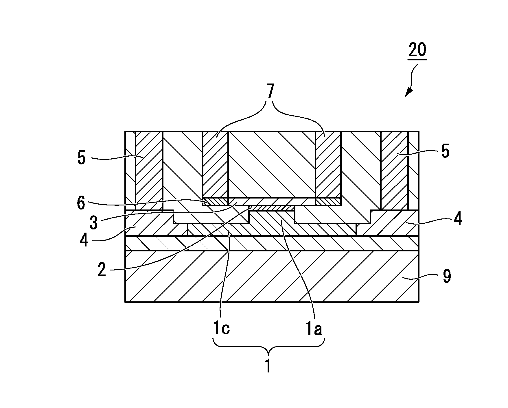
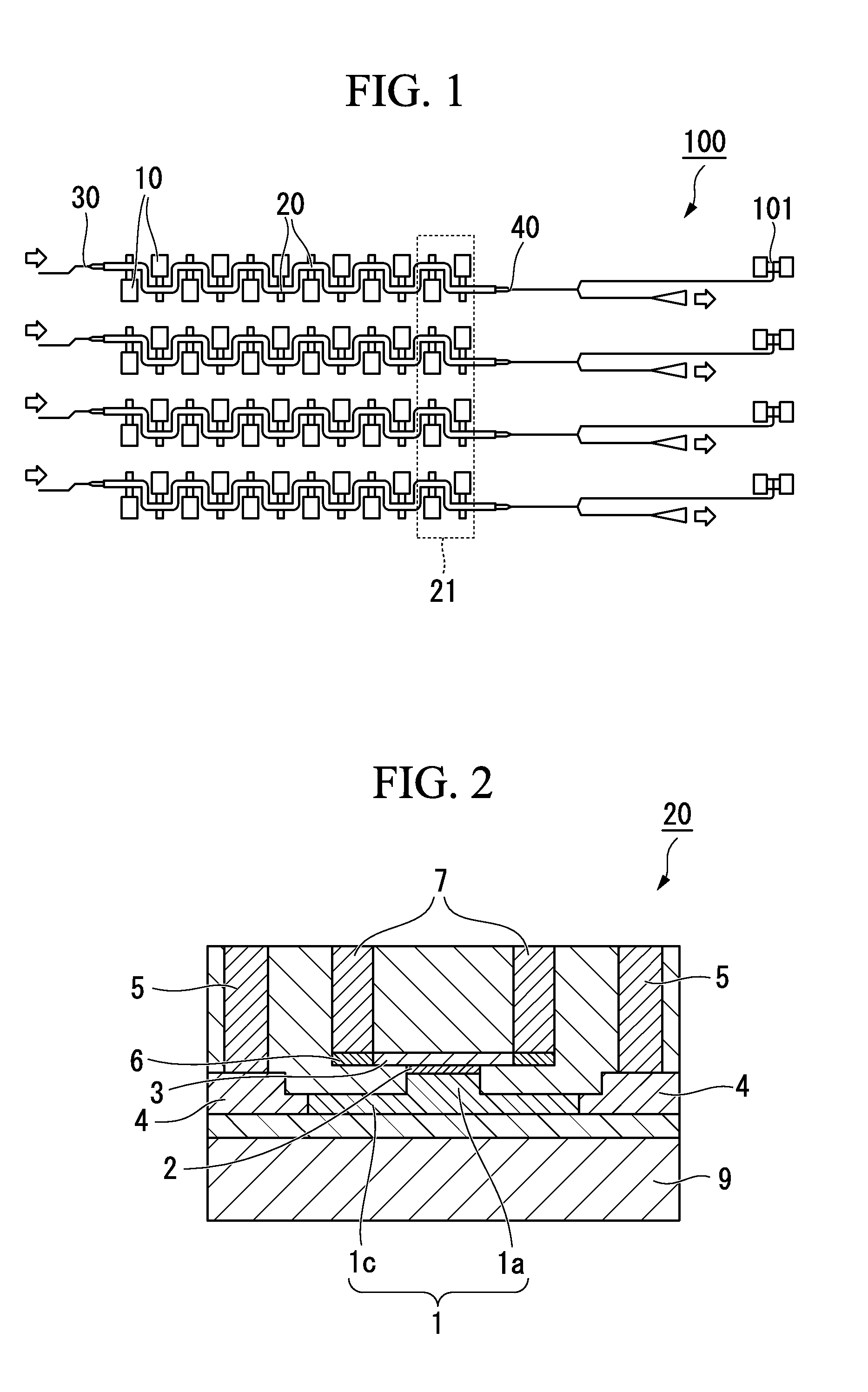
[0046]FIG. 1 is a schematic illustration of an optical modulator 100 according to one embodiment of the present invention. FIG. 2 is a cross-sectional view of a silicon-base electro-optic element forming each of two arms in the optical modulator 100.

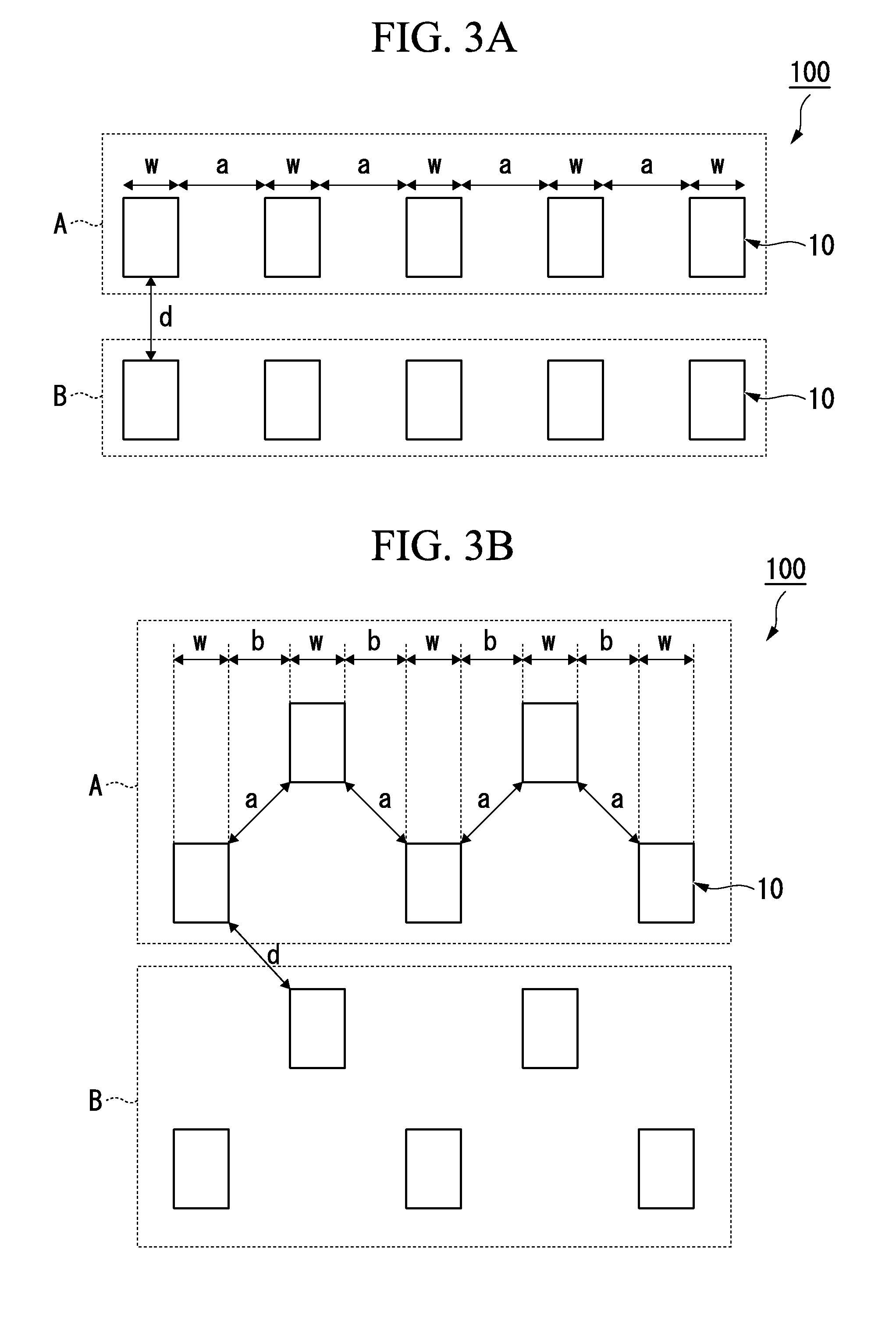
[0047]The optical modulator 100 includes a plurality of electrode pads 10 in a zigzag alignment, two arms 20, an optical branch structure 30 branching two arms 20 in the light-input side, and an optical coupling structure 40 aggregating two arms 20 in the light-output side. Two arms 20 are each bent and folded to circumvent the electrode pads 10. Additionally, two arms 20 are each configured to carry out optical phase modulation at multiple points.

[0048]Two arms 20 are made of silicon-base electro-optic elements as shown in FIG. 2. The silicon-base electro-optic element includes a substrate 9, a first conductive ...


PUM

PropertyMeasurementUnit
wavelengthsaaaaaaaaaa
widthaaaaaaaaaa
thicknessaaaaaaaaaa

Abstract

An optical modulator includes a plurality of electrode pads arranged in a zigzag alignment; two arms which are partially bent to circumvent the electrode pads so as to carry out optical phase modulation at various parts based on voltages input via the electrode pads; an optical branch structure branching the arms; and an optical coupling structure aggregating the arms together. Each arm is made of a silicon-base electro-optic element including a substrate; a first conductive semiconductor layer having a rib waveguide structure; a dielectric layer deposited on the rib waveguide structure; and a second conductive semiconductor layer deposited on the dielectric layer. The first conductive semiconductor layer is connected to first electrode wires via first contacts, while the second conductive semiconductor layer is connected to second electrode wires via second contacts. Thus, it is possible to miniaturize the optical modulator which can operate at a low voltage.

Description

BACKGROUND OF THE INVENTION[0001]1. Field of the Invention[0002]The present invention relates to an optical modulator and an optical modulation device.[0003]The present application claims priority on Japanese Patent Application No. 2014-67114, the entire content of which is incorporated herein by reference.[0004]2. Description of the Related Art[0005]Optical communication devices operating with wavelengths ranging from 1,310 nm to 1,550 nm have been used for local area networks (LANs) and optical fibers used for household appliances. It is preferable to employ silicon-base optical communication devices in which optical function devices and electronic circuits can be integrated on silicon platforms by way of CMOS technologies.[0006]Silicon-base optical communication devices have been developed and applied to waveguides, optical couplers, wavelength filters, optical modulators, etc. Among them, optical modulators serving as active devices have attracted attention among engineers. Addi...

Claims


Application Information

Patent Timeline
Patent Type & Authority Applications(United States)
IPC IPC(8): G02F1/025
CPCG02F1/025G02F1/225
Inventor FUJIKATA, JUNICHITAKAHASHI, SHIGEKI
Owner NEC CORP
Why Eureka
Try Eureka