Device substrate and fabricating method thereof

a technology of device substrate and fabricating method, which is applied in the direction of photomechanical equipment, instruments, photosensitive material processing, etc., can solve the problems of limited adjustment range of exposure amount, phase shift mask, half tone mask, gray tone mask further faces problems, etc., and achieves favorable level difference control capability.

Active Publication Date: 2015-10-15
AU OPTRONICS CORP
View PDF4 Cites 14 Cited by
  • Summary
  • Abstract
  • Description
  • Claims
  • Application Information

AI Technical Summary

Benefits of technology

[0007]The invention provides a device substrate and a fabricating method thereof, which fabricate main spacers and secondary spacers having different heights with use of a general mask and have favorable level difference control capability.
[0011]Based on the above, in addition to using a general mask as a shielding mask for performing front exposure on the photoresist material layer, the patterned light-shielding layer can serve as the shielding mask for performing back exposure on the photoresist material layer, wherein the photoresist material layer may be a negative or positive photoresist. Accordingly, by combining the steps of front exposure, back exposure, non-exposure, and development with different exposure doses (saturated / unsaturated exposure) or different wavelengths, main spacers and secondary spacers having different heights can be fabricated and favorable level difference (i.e. height difference) control capability can be achieved. Thus, the device substrate and the fabricating method of the invention have advantages of lower production costs and simpler fabricating processes.

Problems solved by technology

However, the control capability of the level difference is limited to the stability of the phase shift mask, half tone mask, or gray tone mask at low penetration.
Besides, because the transmittance of the phase shift mask, half tone mask, or gray tone mask is a fixed value after the mask is completed at the factory, the adjustable range of the exposure amount is also limited.
In addition, the phase shift mask, half tone mask, or gray tone mask further faces problems such as high production costs and longer stock preparation time, etc.

Method used


Image

  • Device substrate and fabricating method thereof
  • Device substrate and fabricating method thereof
  • Device substrate and fabricating method thereof

Examples


first embodiment

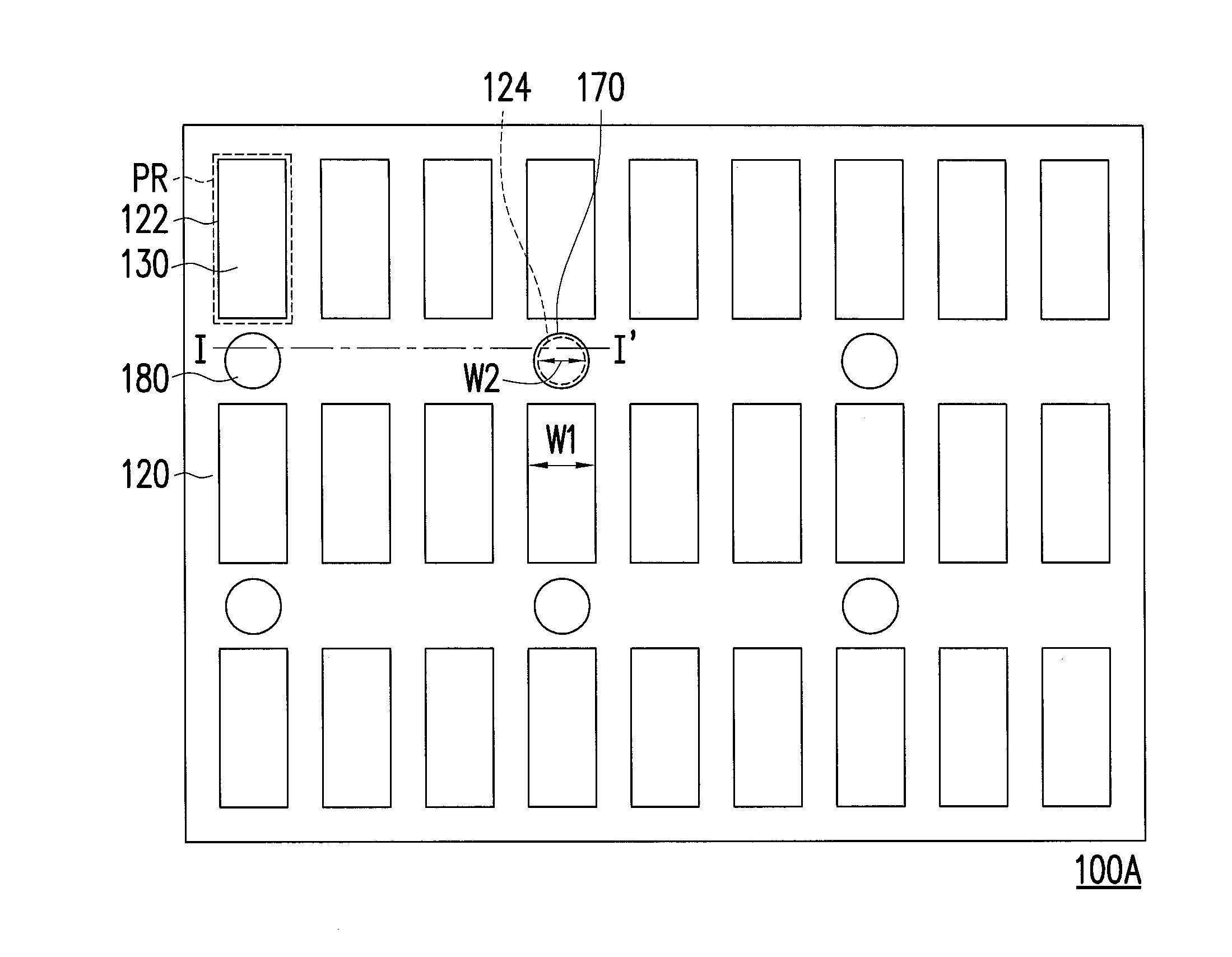
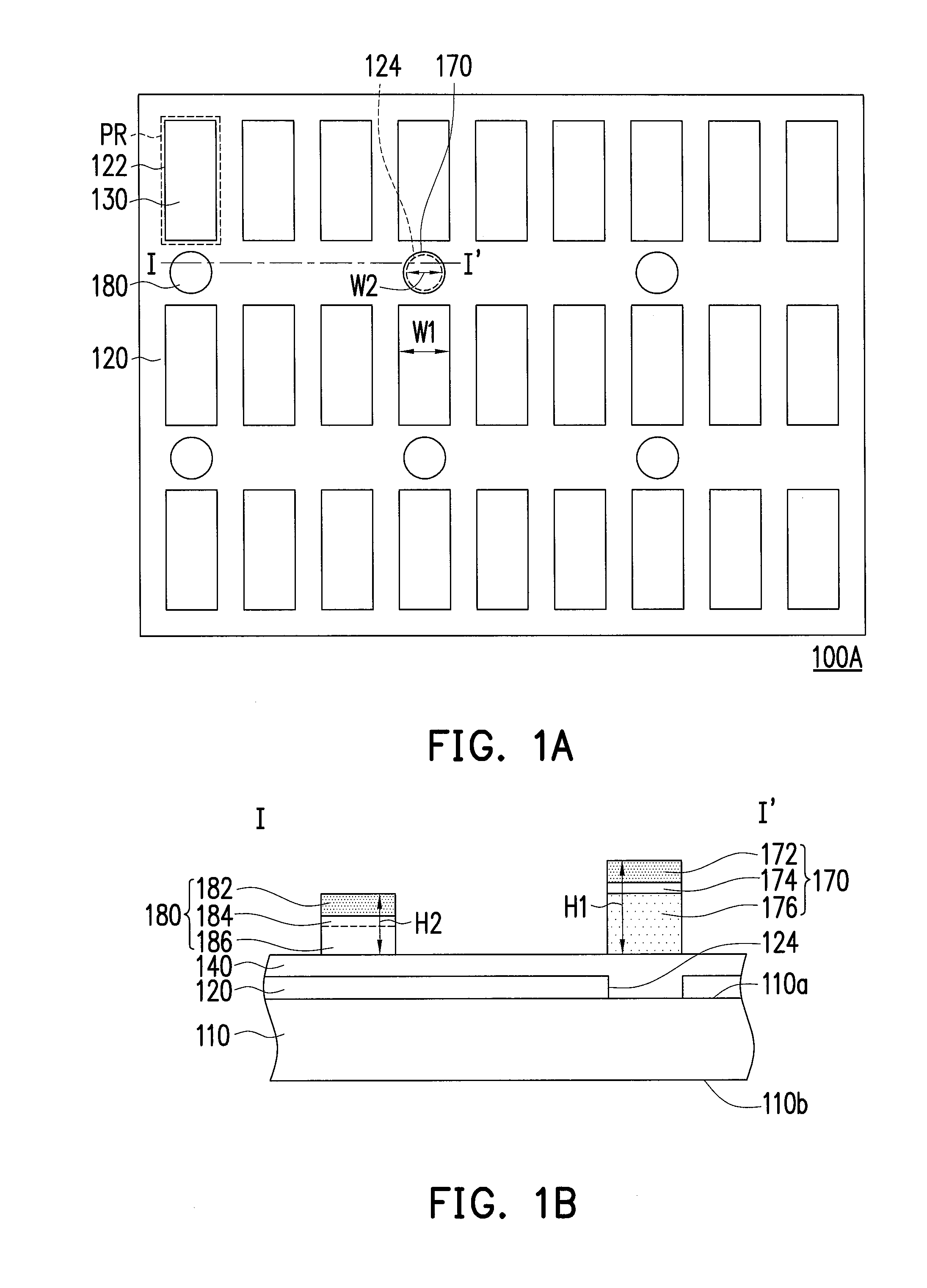
[0039]FIG. 1A is a schematic top view of a device substrate according to the invention. FIG. 1B is a schematic cross-sectional view of the device substrate of FIG. 1A along the line I-I′. In this embodiment, a device substrate 100A is a color filter substrate, an opposite substrate, an active device array substrate, or other suitable device substrates, for example. In the following paragraphs, the device substrate 100A is for example a color filter substrate of a touch display panel in the embodiment of the invention. However, it is noted that the invention is not limited thereto. A display panel of the touch display panel is a liquid crystal display panel, an organic light emitting diode display panel, an electrophoretic display panel, or a plasma display panel, for example.

[0040]With reference to FIG. 1A and FIG. 1B, the device substrate 100A includes a plurality of sub-pixel regions that are arranged in a matrix. Moreover, the device substrate 100A includes a substrate 110, a pat...

second embodiment

[0062]FIG. 3A is a schematic top view of a device substrate according to the invention. FIG. 3B is a schematic cross-sectional view of the device substrate of FIG. 3A along the line I-I′. The embodiment of FIG. 3A to FIG. 3B is similar to the embodiment of FIG. 1A to FIG. 1B. Therefore, identical or similar elements are denoted by the same or similar reference numerals, which will not be described again hereinafter. With reference to FIG. 3A and FIG. 3B, a difference between the embodiment of FIG. 3A to FIG. 3B and the embodiment of FIG. 1A to FIG. 1B is that: in a device substrate 200A, a material of first spacers 270 and second spacers 280 is a positive photoresist, and the height H2 of each of the second spacers 280 is larger than the height H1 of each of the first spacers 270.

[0063]A plurality of the first spacers 270 are disposed on the substrate 110, and vertical projections of the first spacers 270 respectively overlap the first exposure openings 124. More specifically, the f...

third embodiment

[0078]FIG. 6A is a schematic top view of a device substrate according to the invention. FIG. 6B is a schematic cross-sectional view of the device substrate of FIG. 6A along the line I-I′. The embodiment of FIG. 6A to FIG. 6B is similar to the embodiment of FIG. 1A to FIG. 1B. Therefore, identical or similar elements are denoted by the same or similar reference numerals, which will not be described again hereinafter. With reference to FIG. 6A and FIG. 6B, a difference between the embodiment of FIG. 6A to FIG. 6B and the embodiment of FIG. 1A to FIG. 1B is that: in a device substrate 100B, each of the first spacers 170 has a first portion 170a and a second portion 170b connected with a periphery of the first portion 170a, and a height H1 of the first portion 170a is larger than a height H1′ of the second portion 170b.

[0079]A plurality of the first spacers 170 and a plurality of the second spacers 180 are disposed on the substrate 110. Each of the first spacers 170 has the first porti...


PUM

PropertyMeasurementUnit
widthaaaaaaaaaa
widthaaaaaaaaaa
heightaaaaaaaaaa

Abstract

A device substrate and a fabricating method thereof are provided. The device substrate includes a substrate and a patterned light-shielding layer. The patterned light-shielding layer having a plurality of pixel openings and a plurality of first exposure openings is disposed on the substrate, and an area and / or shape of one of the first exposure openings is different from an area and / or shape of one of the pixel openings.

Description

CROSS-REFERENCE TO RELATED APPLICATION[0001]This application claims the priority benefit of Taiwan application serial no. 103113206, filed on Apr. 10, 2014. The entirety of the above-mentioned patent application is hereby incorporated by reference herein and made a part of this specification.BACKGROUND OF THE INVENTION[0002]1. Field of the Invention[0003]The invention relates to a device substrate and a fabricating method thereof, and more particularly relates to a device substrate having exposure openings and a fabricating method thereof.[0004]2. Description of Related Art[0005]As information technology, wireless mobile communication, and information appliances rapidly develop in the recent years, the input devices for a great many information products have been changed from the conventional keyboards or mice to touch display panels for the purposes of convenience, miniaturization, and being user-friendly. Especially, the touch display panel has become the most popular product amon...

Claims


Application Information

Patent Timeline
Patent Type & Authority Applications(United States)
IPC IPC(8): G02B5/20G03F7/20G02B5/00
CPCG02B5/20G03F7/20G02B5/003G02B5/201G02F1/133516G02F1/13394G03F7/0007G03F7/027G03F7/038G03F7/2022G02F1/13396G03F7/32
Inventor PEI, KAI
Owner AU OPTRONICS CORP
Why Eureka
Try Eureka