
Liquid crystal display device, substrate for liquid crystal display device and manufacturing method of substrate for liquid crystal display device

a technology of liquid crystal display device and substrate, which is applied in the direction of static indicating device, instruments, optical elements, etc., can solve the problems of difficult to implement in-cell electro capacitive touch sensing, irregular display, and inconvenience for observers

Active Publication Date: 2015-10-22
TOPPAN PRINTING CO LTD
View PDF2 Cites 68 Cited by
  • Summary
  • Abstract
  • Description
  • Claims
  • Application Information

AI Technical Summary

Benefits of technology

The present invention is about a liquid crystal display screen that can display 2D or 3D images. This patent is also about a special way to make a substrate for this display screen that allows for the creation of 3D displays.

Problems solved by technology

In methods using glasses, the observer is required to wear dedicated glasses, which causes discomfort to the observer.
However, in patent literature 1, by a pixel arrangement in which pixels are arranged substantially in oblique and an edge of the lenticular screen that intersects this pixel arrangement, irregularities may occur on the display.
According to the configuration of the parallax barrier described in the patent literature 9, since the parallax barrier is electrically conductive, it is difficult to implement in-cell type electro capacitive touch sensing.
According to a film forming method of the parallax barrier in the patent literature 9, it is considered that high manufacturing cost will be required.
Thus, in a case where the black matrix and the parallax barrier have the light shielding properties, performing a photo alignment may be difficult.

Method used


Image

  • Liquid crystal display device, substrate for liquid crystal display device and manufacturing method of substrate for liquid crystal display device
  • Liquid crystal display device, substrate for liquid crystal display device and manufacturing method of substrate for liquid crystal display device
  • Liquid crystal display device, substrate for liquid crystal display device and manufacturing method of substrate for liquid crystal display device

Examples


first embodiment

[0061]In the present embodiment, the pixel has a long side along the longitudinal direction.

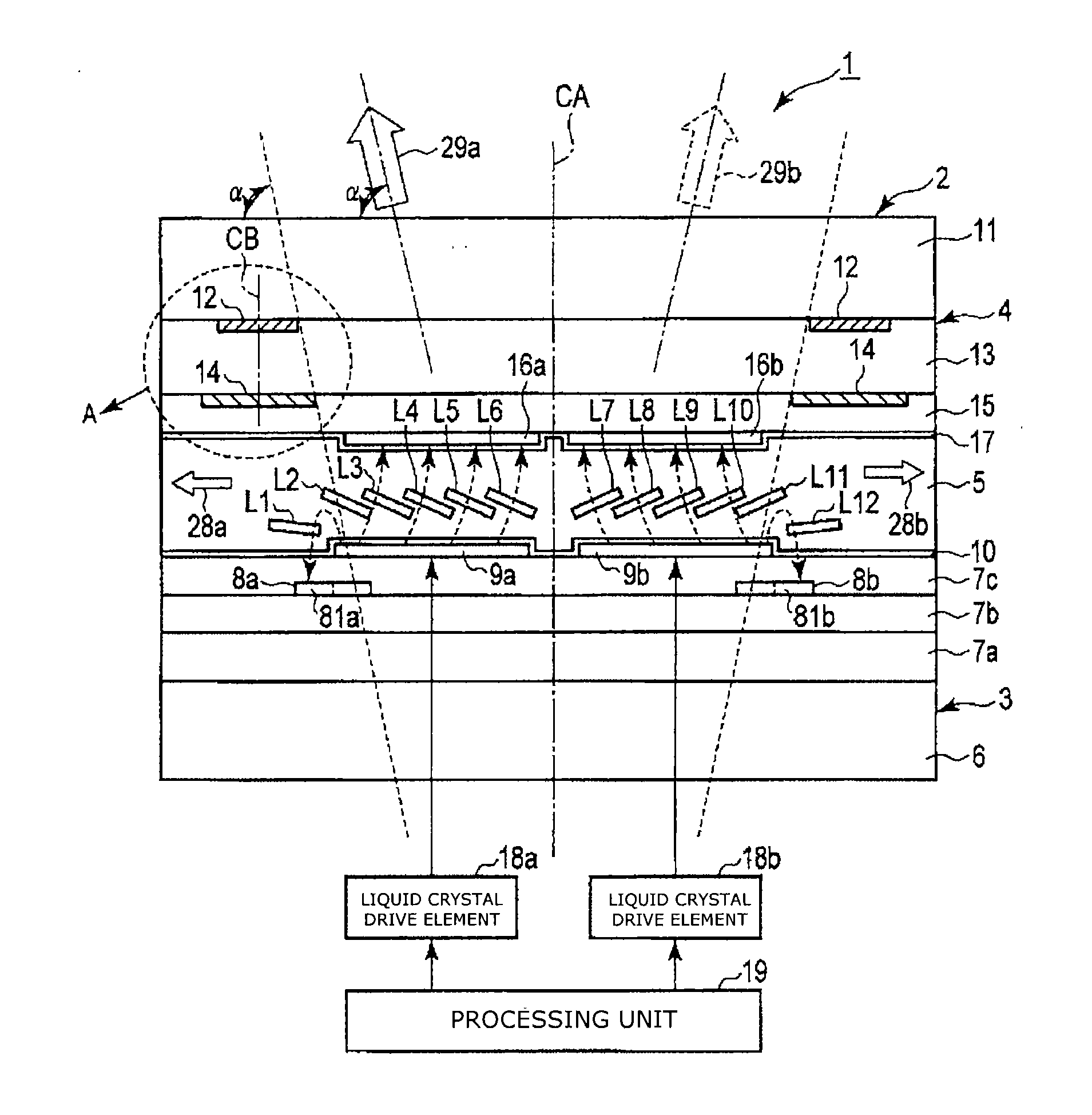
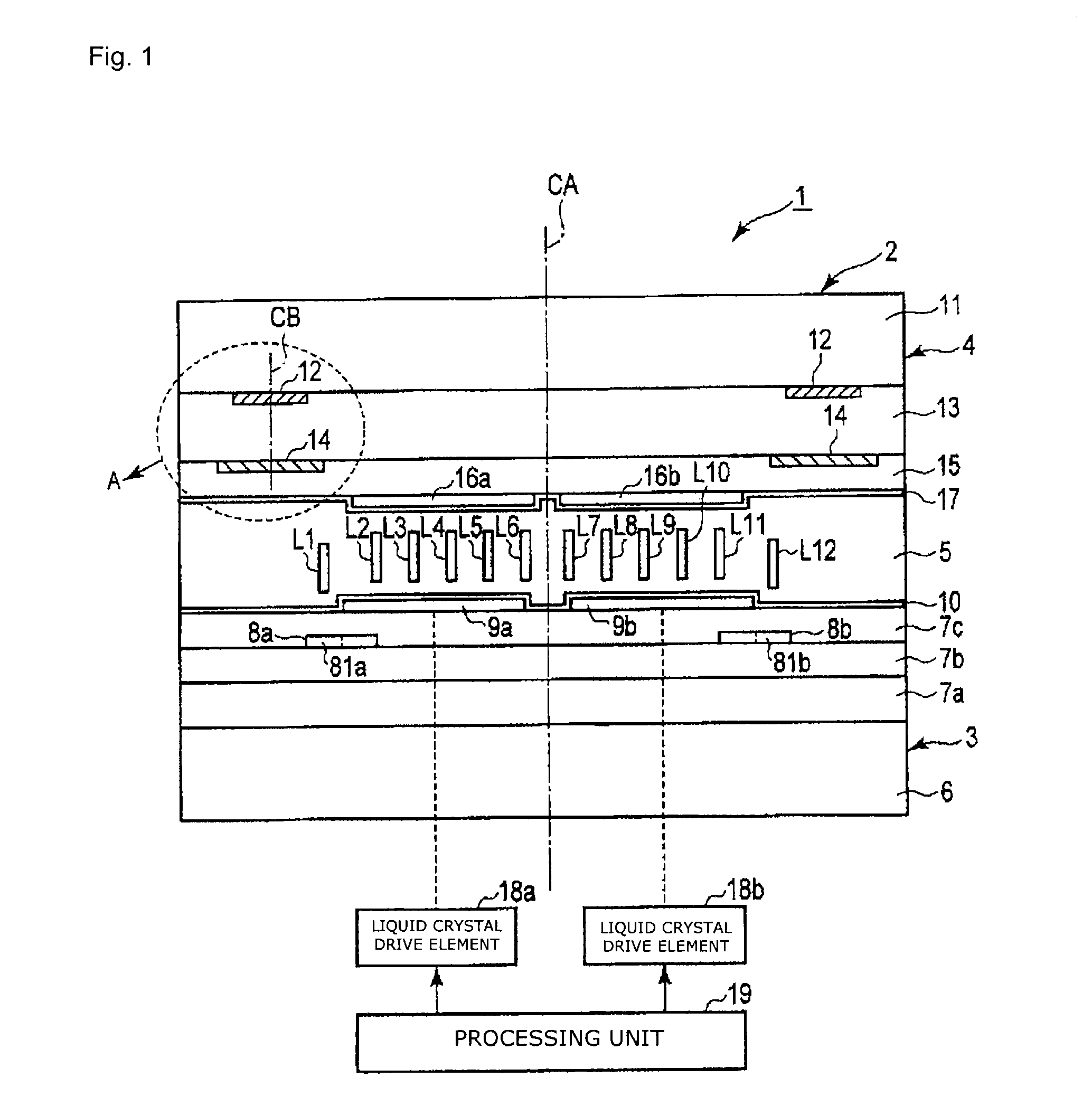
[0062]FIG. 1 is a partial cross sectional view showing an example of a configuration of a liquid crystal panel 2 provided in the liquid crystal display device 1 according to the present embodiment. FIG. 1 is a cross sectional view in the horizontal direction of a pixel of the liquid crystal display panel 2. In FIG. 1, a pixel having a long side along the longitudinal direction represents a pixel having a longitudinal direction in a direction perpendicular with respect to the plane of the paper. FIG. 1 illustrates an example of a state where the liquid crystal drive voltage is not applied. In the liquid crystal panel 2, a polarizing plate and a phase difference plate or the like are omitted.

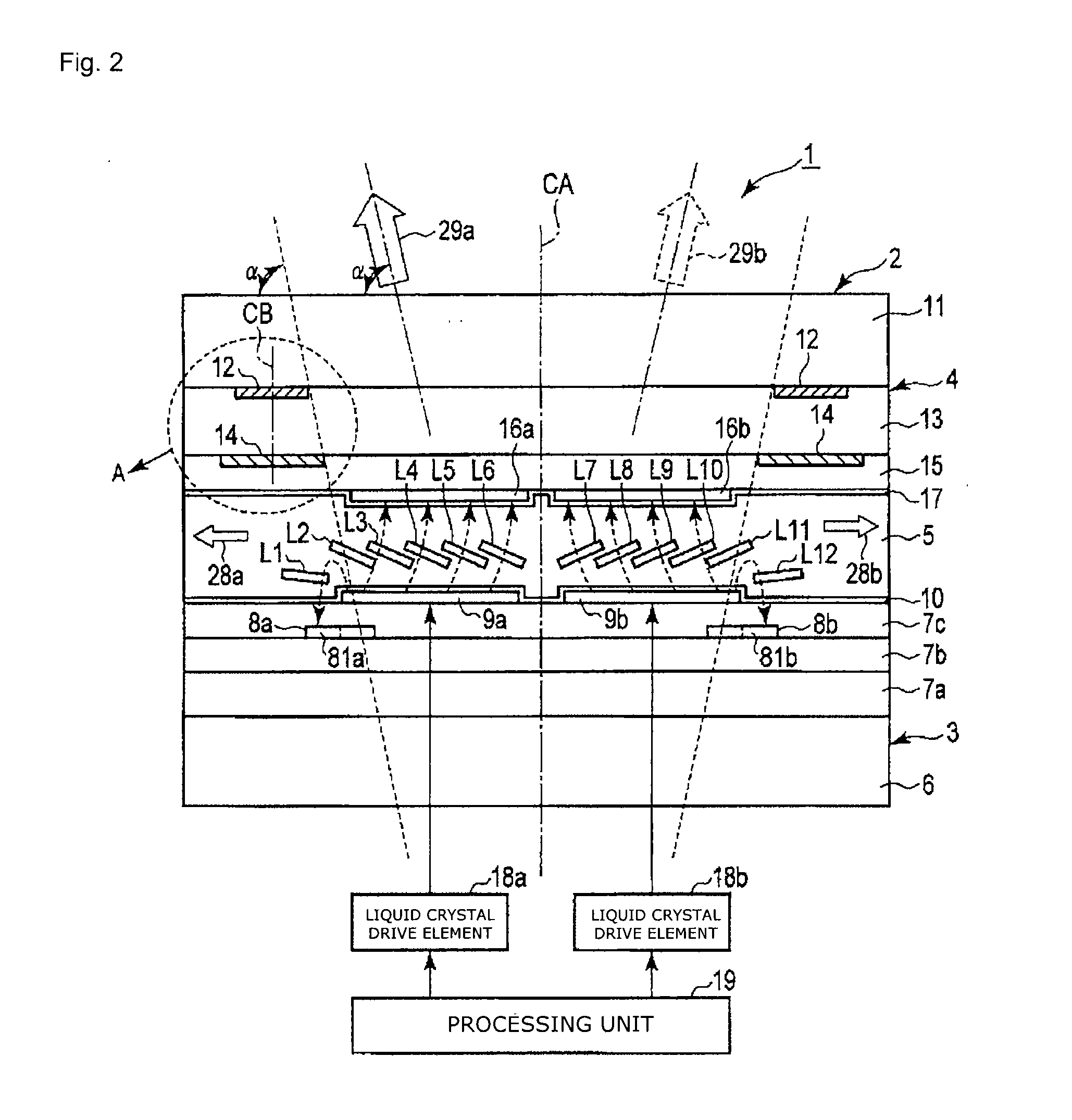
[0063]FIG. 2 is a partial cross sectional view of showing an example of a state of the liquid crystal panel 2 when the liquid crystal drive voltage is supplied.

[0064]In the present embodiment, a case is des...

second embodiment

[0189]In the present embodiment, a flow chart shows an example of manufacturing step concerning the manufacturing method of the counter substrate 4 according to the above-described first embodiment.

[0190]FIG. 14 is a flowchart showing an example of a manufacturing method of a counter substrate 4 according to the present embodiment.

[0191]At step S1, a light shielding color material containing carbon pigment as a principal component is coated on the transparent substrate 11, exposed and then developed. Thus, the carbon pigment light shielding layer 12 and alignment marks are formed. In step S1, as a manufacturing apparatus, a coating apparatus, a drying machine, an exposure apparatus, a development apparatus, and a cured film apparatus are used. As a representative drying machine and cured film apparatus, a clean oven and a hot plate are used.

[0192]At step S2, by using the coating apparatus and the cured film apparatus, the first transparent resin layer 13 is formed.

[0193]At step S3, ...

third embodiment

[0219]According to the third embodiment, a liquid crystal display device is described in which a color filter used for a color display is provided in the counter substrate 4 according to the above-described first and second embodiments. In the present embodiment, a colored pixel has a shape extending in the longitudinal direction. The pixel includes any of a red filter, green filter or blue filter. It should be noted that two sub pixels having identical color may be a single pixel.

[0220]FIG. 16 is a partial cross sectional view showing an example of a configuration of a liquid crystal panel 32 provided in the liquid crystal display device 31 according to the present embodiment. FIG. 16 is a cross-sectional view sectioned across the horizontal direction (pixel width direction) of the pixel of the liquid crystal panel 32. FIG. 16 illustrates a state under a condition in which the liquid crystal drive voltage is applied. In the liquid crystal panel 32, a polarizing plate and a phase di...


PUM

PropertyMeasurementUnit
Angleaaaaaaaaaa
Dielectric anisotropyaaaaaaaaaa
Shapeaaaaaaaaaa

Abstract

A liquid crystal display device includes a counter substrate facing an array substrate via a liquid crystal layer, and a backlight unit provided on a back side of the array substrate. The counter substrate includes a first light shielding layer formed on a first transparent substrate, a transparent resin layer formed on the first transparent substrate, and a second light shielding layer formed on the transparent resin layer. The first light shielding layer has openings corresponding to polygonal pixels having a polygonal shape in which at least two edges are parallel in a planar view. The first light shielding layer includes a first linear pattern having a center line that overlaps with a center line of a second linear pattern of the second light shielding layer in a planar view. The first linear pattern has a line width different from a line width of the second linear pattern.

Description

CROSS-REFERENCE TO RELATED APPLICATIONS[0001]The present application is a continuation application of International Application No. PCT / JP2013 / 083624, filed Dec. 16, 2013, which is based upon and claims the benefit of priority to Japanese Patent Application No. 2012-286225, filed Dec. 27, 2012. The entire contents of these applications are incorporated herein by reference.BACKGROUND OF THE INVENTION[0002]1. Field of the Invention[0003]The present invention relates to a liquid crystal display device capable of displaying two dimensional displays or three dimensional (stereo image) displays, a substrate for a liquid crystal display device and a manufacturing method of the substrate for a liquid crystal display device.[0004]2. Discussion of the Background[0005]A liquid crystal panel included in a general liquid crystal display has a configuration in which a liquid crystal layer is sandwiched by two substrates. The two substrates include, for example, a transparent substrate such as gla...

Claims


Application Information

Patent Timeline
IPC IPC(8): G02F1/1335G02B27/22G02F1/1343G02F1/1333G02F1/133G02F1/1368G02B30/27
CPCG02F1/133512G02F1/13318G02F1/1368G02F1/134309G02B27/22G02F1/133602G02F1/13439G02F1/133514G02F1/133516G02F1/133345H04N13/00G02F1/13338G02F1/133615H04N13/30G02B30/27G02F1/133623G02F1/134381G02F1/134345G02F1/134318
Inventor KIMURA, YUKIHIROFUKUYOSHI, KENZO
Owner TOPPAN PRINTING CO LTD
Features
  • Generate Ideas
  • Intellectual Property
  • Life Sciences
  • Materials
  • Tech Scout
  • Unparalleled Data Quality
  • Higher Quality Content
  • 60% Fewer Hallucinations
Learn More