Package structure

a packaging and structure technology, applied in the direction of basic electric elements, electrical apparatus contruction details, association of printed circuit non-printed electric components, etc., can solve the problems of long traces between electronic components, high line impedance, and still have drawbacks of the conventional housing package structure, so as to improve the electrical properties

Active Publication Date: 2015-10-22
DELTA ELECTRONICS INTL SINGAPORE
View PDF0 Cites 33 Cited by
  • Summary
  • Abstract
  • Description
  • Claims
  • Application Information

AI Technical Summary

Benefits of technology

[0006]The present invention provides a package structure with a direct bond copper (DBC) substrate partially em

Problems solved by technology

Although the DBC substrate may provide good heat-dissipating efficacy and withstand higher voltage, the conventional housing package structure still has some drawbacks.
Moreover, since the electronic components are arranged on the same layer of the DBC substrate, the traces between the ele

Method used


Image

  • Package structure
  • Package structure
  • Package structure

Examples


Embodiment Construction

[0021]The present invention will now be described more specifically with reference to the following embodiments. It is to be noted that the following descriptions of preferred embodiments of this invention are presented herein for purpose of illustration and description only. It is not intended to be exhaustive or to be limited to the precise form disclosed.

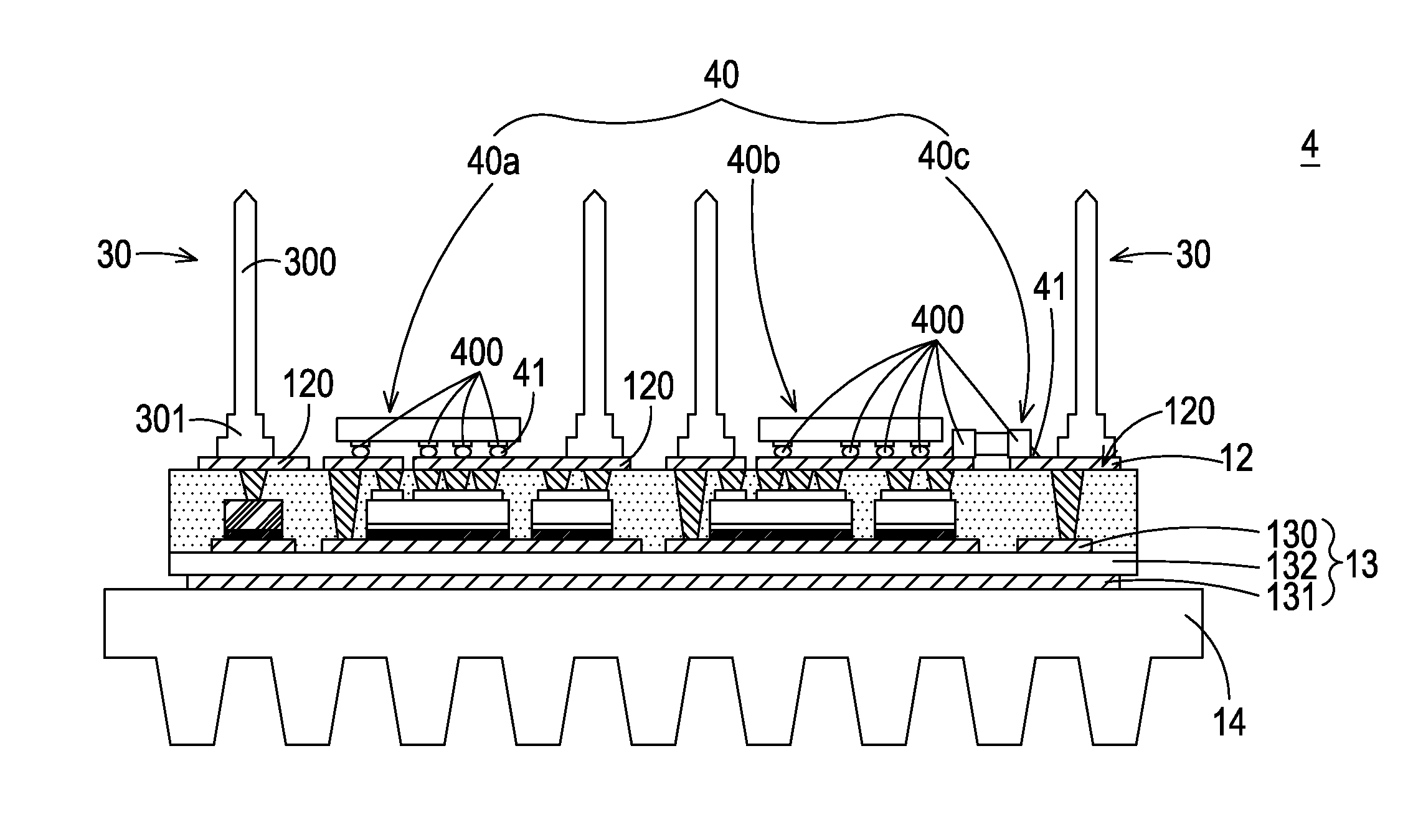
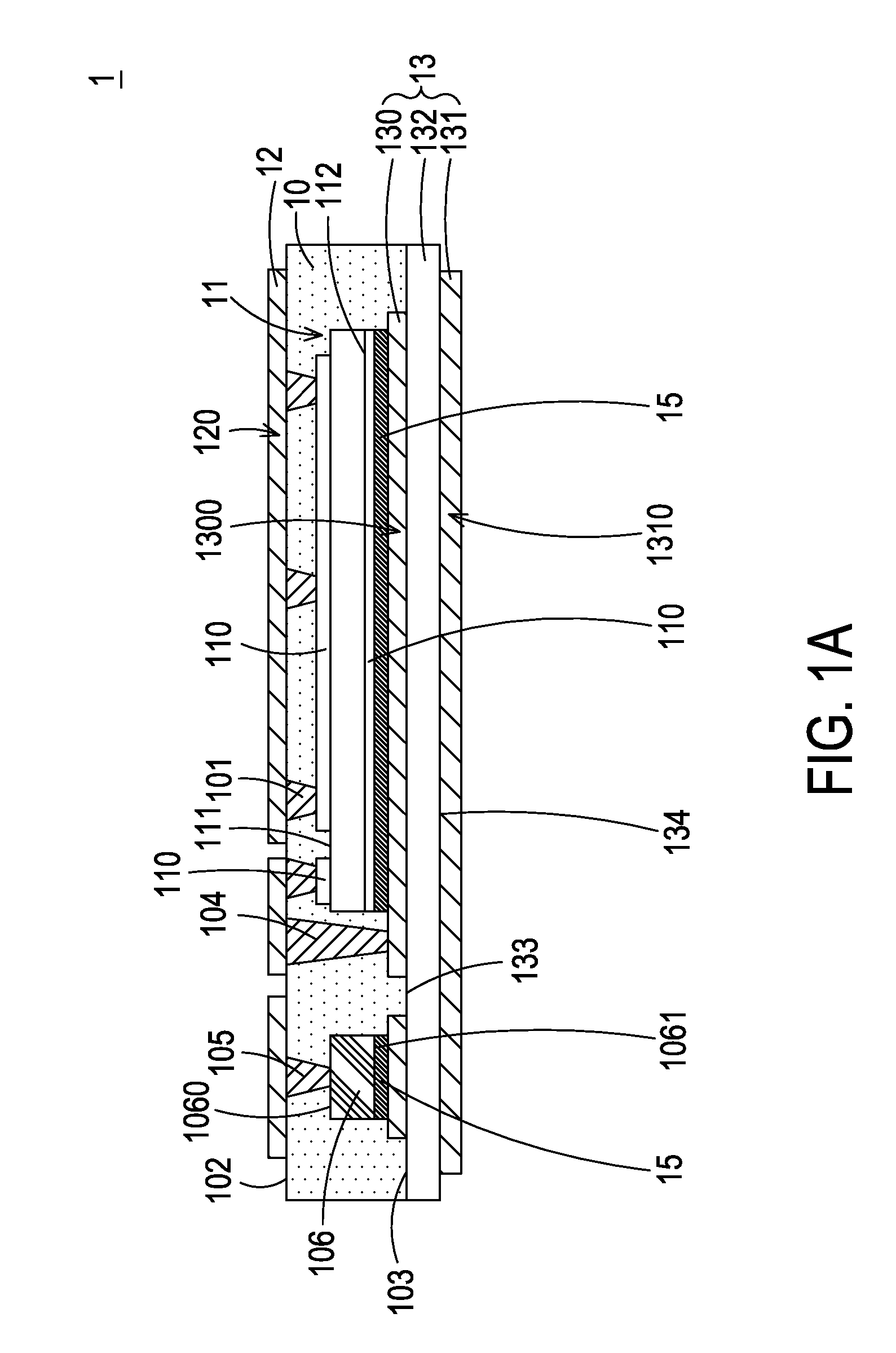
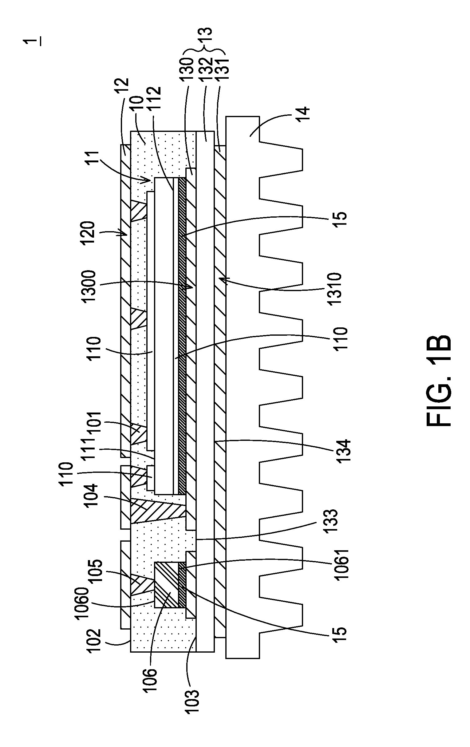
[0022]FIG. 1A is a schematic cross-sectional view illustrating a package structure according to a first embodiment of the present invention. The package structure 1 is a surface mount device (SMD) package structure. As shown in FIG. 1A, the package structure 1 includes a first insulation layer 10, at least one first electronic component 11, a first conductive layer 12, and a direct bond copper (DBC) substrate 13.

[0023]Moreover, a plurality of first conductive vias 101 are formed in the first insulation layer 10. The first conductive layer 12 is disposed on a top surface 102 of the first insulation layer 10. Moreover, a part of th...


PUM


Abstract

A package structure includes a first insulation layer, a first conductive layer, a direct bond copper substrate, and a first electronic component. A first conductive via is formed in the first insulation layer. The first conductive layer is disposed on a top surface of the first insulation layer and in contact with the first conductive via. The direct bond copper substrate includes a second conductive layer, a third conductive layer and a ceramic base. The ceramic base is disposed on a bottom surface of the first insulation layer and exposed to the first insulation layer by press-fit operation. The first electronic component is embedded within the first insulation layer and disposed on the second conductive layer. The first electronic component includes a first conducting terminal. The first conducting terminal is electrically connected with the second conductive layer and/or electrically connected with the first conductive layer through the first conductive via.

Description

FIELD OF THE INVENTION[0001]The present invention relates to a package structure, and more particularly to a package structure with a direct bond copper (DBC) substrate partially embedded within an insulation layer.BACKGROUND OF THE INVENTION[0002]Recently, the general trends in designing electronic devices are toward small size, light weightiness and easy portability. Moreover, with the increasing development of electronic industries, the internal circuitries of the electronic devices are gradually modularized. In other words, several electronic components are integrated into a single circuit module. For example, a power module is one of the widely-used circuit modules. The power module may be applied to an inverter, a converter, an electric vehicle (EV) or a hybrid electric vehicle (HEV). After the electronic components (e.g. capacitors, resistors, inductors, transformers, diodes and transistors) are integrated as a power module, the power module may be installed on a motherboard ...

Claims


Application Information

Patent Timeline
IPC IPC(8): H01L23/00H01L23/15H01L23/36H01L23/522
CPCH01L24/32H01L23/5226H01L23/15H01L24/33H01L2224/0951H01L24/09H01L2224/33055H01L2224/29147H01L23/36H01L2924/13091H01L2924/181H01L23/3735H01L23/49811H01L23/5383H01L23/5389H01L2924/13055H01L2224/73267H01L2224/24226H01L2924/19043H01L2924/19042H01L2224/24195H01L24/24H01L2224/24137H01L24/25H01L2224/12105H01L2924/19105H01L2224/04105H01L2224/16227H01L2924/19041H01L2224/24105H01L2224/06181H01L2924/00H01L2924/00012
Inventor CHEN, DA-JUNG
Owner DELTA ELECTRONICS INTL SINGAPORE
Why Eureka
Try Eureka