Manufacturing method for semi-floating gate device

Active Publication Date: 2015-10-22
SUZHOU ORIENTAL SEMICONDUCTOR CO LTD
View PDF10 Cites 25 Cited by
  • Summary
  • Abstract
  • Description
  • Claims
  • Application Information

AI Technical Summary

Benefits of technology

[0037]Compared with the prior art, the present invention has the following notable advantages.
[0038]Firstly, a floating gate of the present invention is formed by means of two deposition processes, one photolithography process, and two etching processes, and although the number of processes for manufacturing the floating gate is increased, a photolithography process and an etching process for separately forming a floating gate opening region are omitted, so that process procedures for manufacturing a semi-floating gate device with a U-shaped cha

Problems solved by technology

The process procedures of forming a floating gate opening region 204 in the first layer of insulating film 203 on the side wall located on the top of the U-shaped groove and close t

Method used


Image

  • Manufacturing method for semi-floating gate device
  • Manufacturing method for semi-floating gate device
  • Manufacturing method for semi-floating gate device

Examples


Example

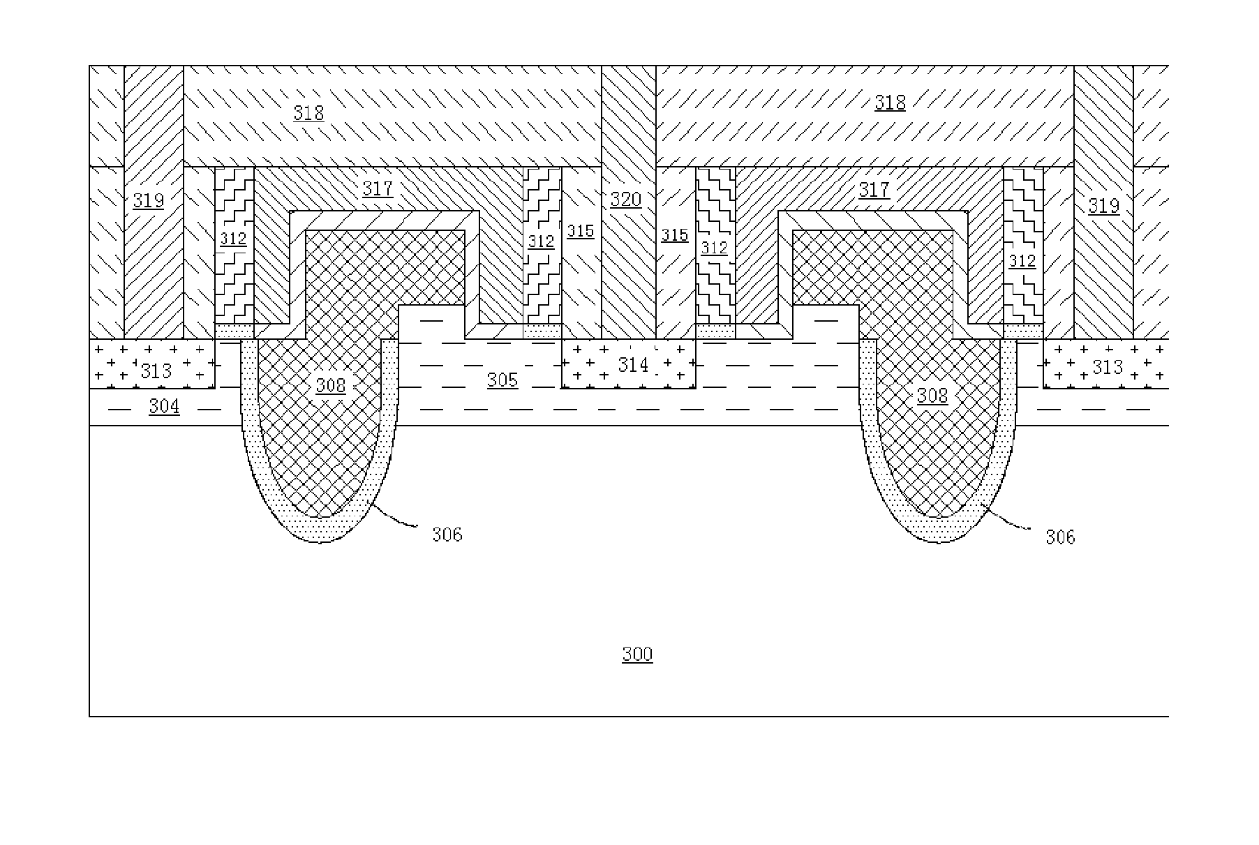
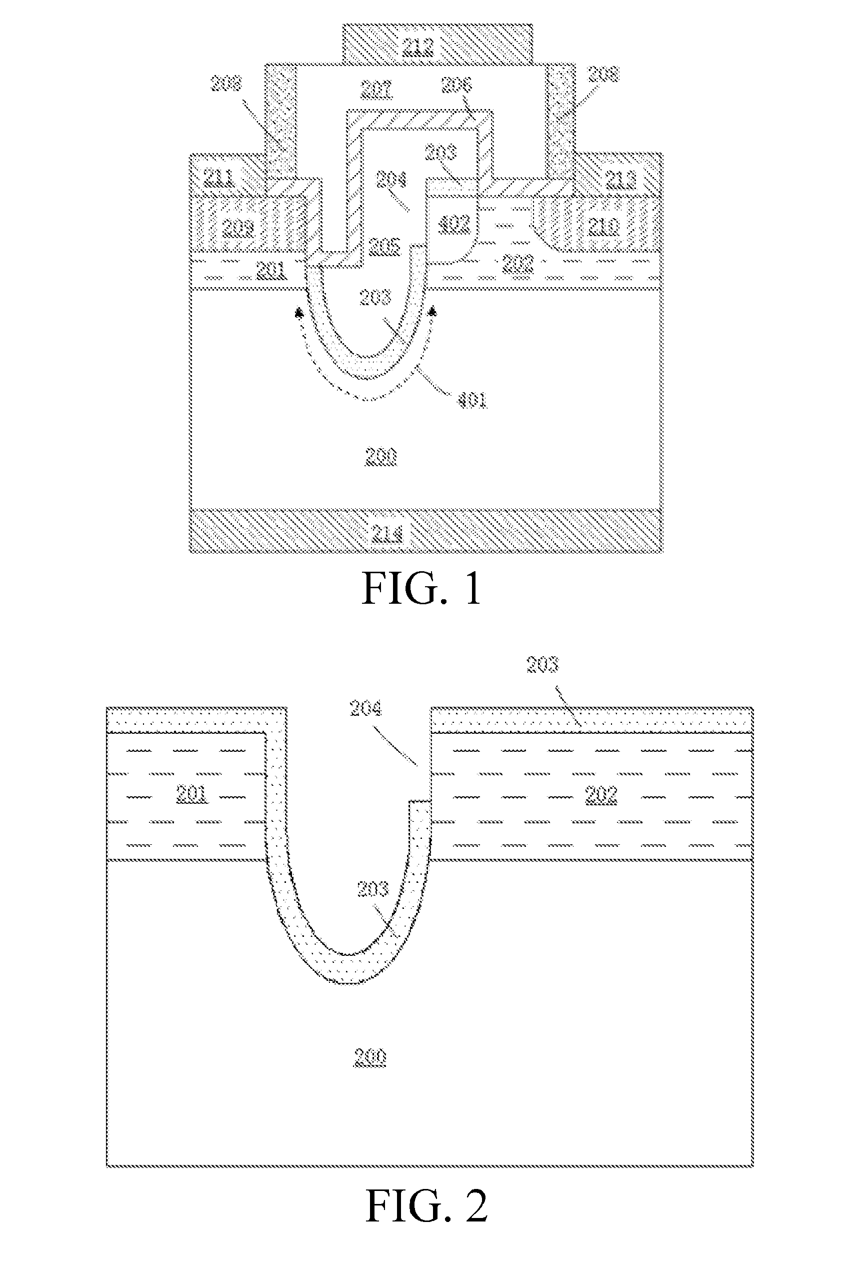
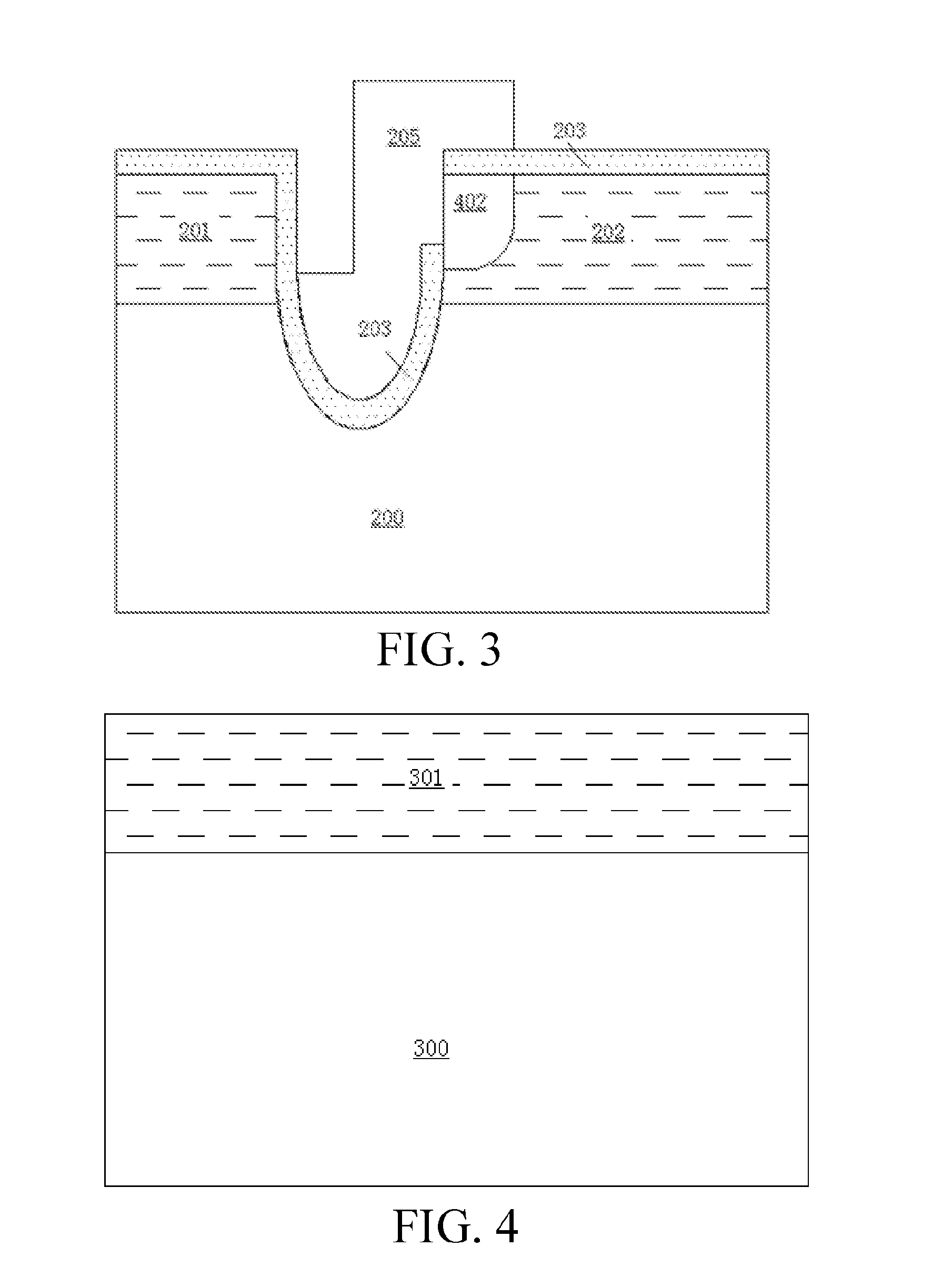
[0045]In order to clearly describe specific implementation manners of the present invention, layers and regions disclosed in the present invention are enlarged in terms of thickness in schematic diagrams listed in the accompanying drawings of the description, and sizes of the schematic diagrams do not represent actual sizes; the accompanying drawings are illustrative and shall not define the scope of the present invention. Embodiments listed in the description shall not be limited to specific shapes of regions shown in the accompanying drawings, but include that an obtained shape, for example, has deviation and the like caused by manufacturing and a curve obtained by etching, for another example, usually has a curving or mellow and full characteristic, but the shapes are all represented by rectangles in the embodiments of the present invention; meanwhile, in the following description, a term in use, namely, a substrate, may be interpreted as a semiconductor wafer which is being proc...


PUM


Abstract

A manufacturing method for a semi-floating gate device, mainly comprising a manufacturing method for a floating gate and a floating gate opening area, and the specific process thereof is: reserving a hard mask layer after a U-shaped groove is formed, growing a gate dielectric layer on a surface of the formed U-shaped groove, depositing and etching back a first layer of polysilicon to protect the gate dielectric layer, etching away the exposed gate dielectric layer and hard mask layer, then covering a formed structure to deposit a second layer of polysilicon, then etching a formed polysilicon layer by a photoetching process and an etching process so as to form a floating gate, and forming a floating gate opening area in a self-aligning way. The manufacturing method can simplify the existing manufacturing process for a semi-floating gate device, reduce the difficulty in manufacturing the semi-floating gate device with a U-shaped channel, and improve the yield of the semi-floating-gate device.

Description

BACKGROUND OF THE INVENTION[0001]1. Field of the Invention[0002]The present invention pertains to the field of semiconductor memory technologies, relates to a method for manufacturing a dynamic random access memory and in particular, relates to a method for manufacturing a semi-floating gate device.[0003]2. Description of Related Art[0004]Semiconductor memories are widely used in many electronic products. There are different requirements for the construction, performance, and density of the semiconductor memory in different application fields. For example, a static random access memory (SRAM) has a very high random access speed and a relatively low integration density, while a standard dynamic random access memory (DRAM) has a very high integration density and a moderate random access speed. Currently, with the continuous expansion of the market demand for semiconductor memories, the processes and methods for manufacturing dynamic random access memory technologies are innovated and ...

Claims


Application Information

Patent Timeline
IPC IPC(8): H01L27/115H01L29/861H01L29/739H01L29/51H01L29/10H01L29/423H01L29/49H01L29/788H01L27/06
CPCH01L27/11521H01L29/788H01L29/861H01L29/7391H01L27/0629H01L29/42364H01L29/42336H01L29/4916H01L29/517H01L29/518H01L29/1037H01L21/28H01L29/42324H10B41/00H10B69/00H01L29/66825H01L27/0727H01L29/7881H01L29/40114H10B41/30
Inventor LIU, WEILIU, LEI
Owner SUZHOU ORIENTAL SEMICONDUCTOR CO LTD
Why Eureka
Try Eureka