Silicon photonics device and communication system therefor

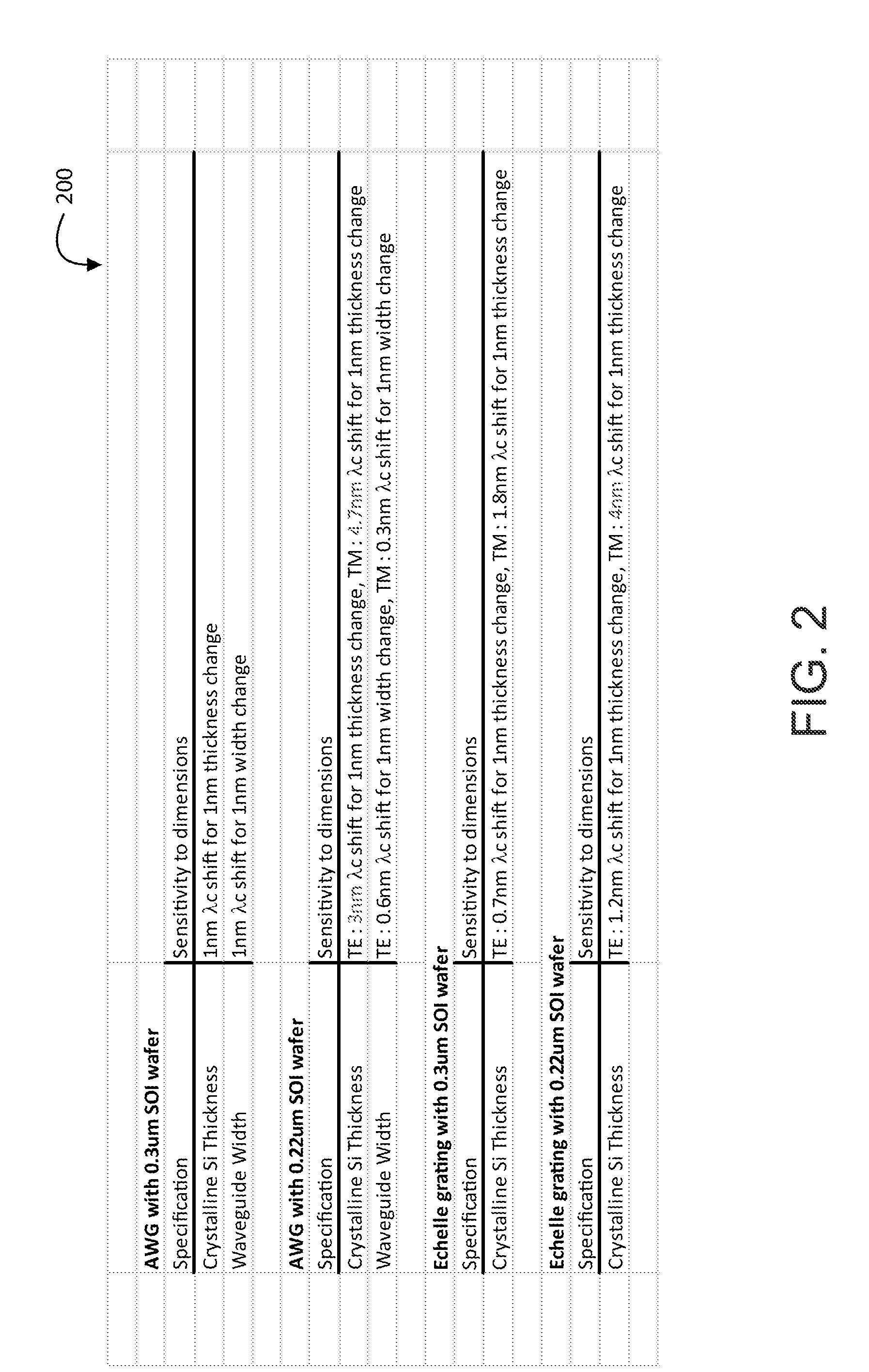
a technology of silicon photonics and communication systems, applied in the field of telecommunication techniques and integrated circuit devices, can solve the problems of large bandwidth, large amount of data transferred, and limited popular applications, and achieve the effect of reducing the sensitivity to thickness changes in crystalline silicon thickness and/or waveguide width

Active Publication Date: 2015-10-29
MARVELL ASIA PTE LTD
View PDF9 Cites 25 Cited by
  • Summary
  • Abstract
  • Description
  • Claims
  • Application Information

AI Technical Summary

Benefits of technology

[0009]Many benefits are recognized through various embodiments of the present invention. Such benefits include reduced sensitivity to thickness changes in crystalline silicon thickness and and / or waveguide width. Silicon photonics devices using the 300 nm SOI wafer can be characterized by polarization independence and can be substantially free of polarization dependent wavelength shifts. Using symmetric waveguide geometry, light signals can be transmitted being substantially free from time delays between TE and TM light. Other benefits will be recognized by those of ordinary skill in the art that the mechanisms described can be applied to other communications systems as well.

Problems solved by technology

In the early days of the Internet, popular applications were limited to emails, bulletin board, and mostly informational and text-based web page surfing, and the amount of data transferred was relatively small.
Today, Internet and mobile applications demand a huge amount of bandwidth for transferring photo, video, music, and other multimedia files.
These limitations provide significant challenges to the continued improvement of communication systems scaling and performance.
Unfortunately, they have been inadequate for various applications.

Method used


Image

  • Silicon photonics device and communication system therefor
  • Silicon photonics device and communication system therefor
  • Silicon photonics device and communication system therefor

Examples


Embodiment Construction

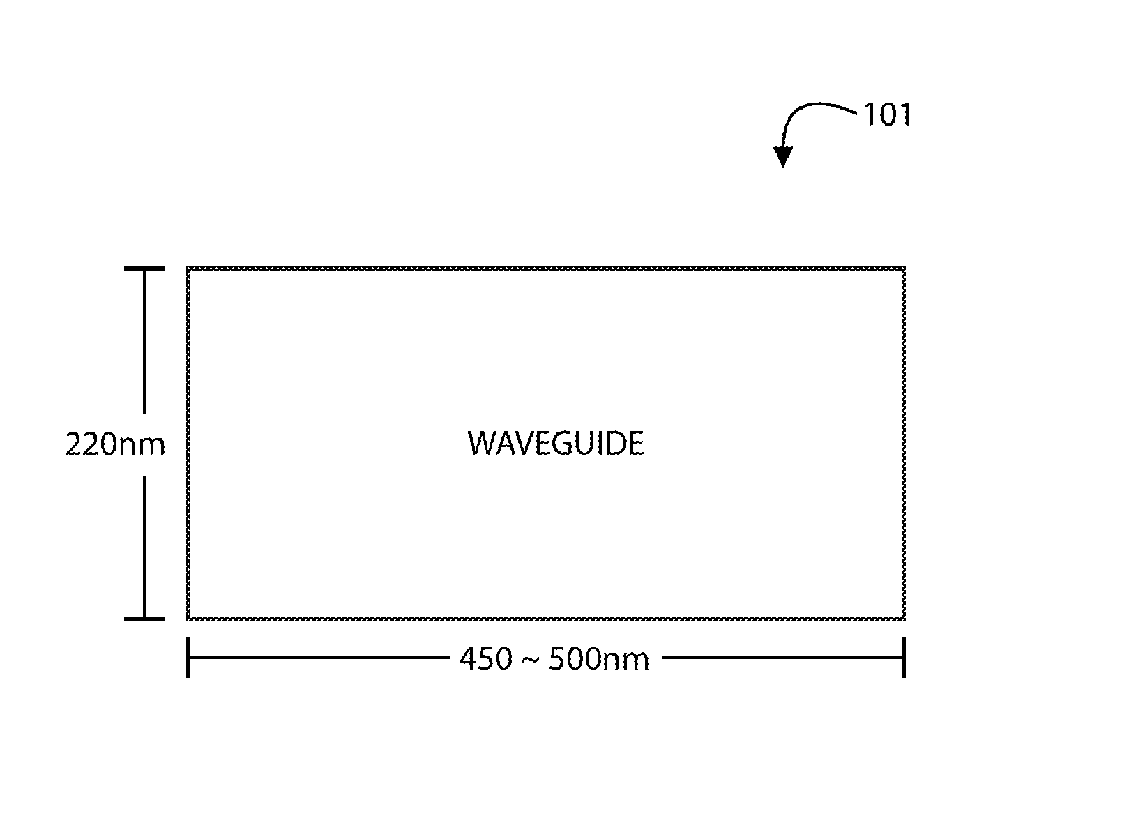
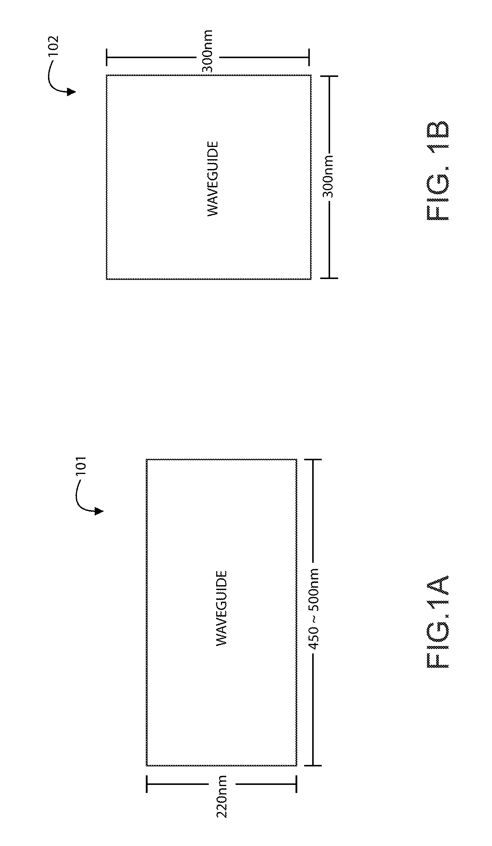
[0022]The present invention relates to telecommunication techniques and integrated circuit (IC) devices. More specifically, various embodiments of the present invention provide integrated silicon photonics devices.

[0023]The following description is presented to enable one of ordinary skill in the art to make and use the invention and to incorporate it in the context of particular applications. Various modifications, as well as a variety of uses in different applications will be readily apparent to those skilled in the art, and the general principles defined herein may be applied to a wide range of embodiments. Thus, the present invention is not intended to be limited to the embodiments presented, but is to be accorded the widest scope consistent with the principles and novel features disclosed herein.

[0024]In the following detailed description, numerous specific details are set forth in order to provide a more thorough understanding of the present invention. However, it will be appa...


PUM


Abstract

A silicon photonics device and system therefor. The silicon photonics device can include a 300 nm SOI (silicon-on-insulator with 300 nm top Si) overlying a substrate member. A waveguide structure can be configured from a portion of the SOI layer and disposed overlying the substrate member. This waveguide structure can include an AWG (Arrayed Waveguide Gratings) structure with 300 nm×300 nm symmetric grating waveguides or an Echelle grating structure characterized by a top silicon thickness of 300 nm. The waveguide structure can also include an index compensator material configured to provide at least two material index ratings in the waveguide structure.

Description

CROSS-REFERENCE TO RELATED APPLICATIONS[0001]N / ABACKGROUND OF THE INVENTION[0002]The present invention relates to telecommunication techniques and integrated circuit (IC) devices. More specifically, embodiments of the present invention provide a silicon photonics device having improved wavelength sensitivity to device dimensions and a communication interface using the silicon photonics device.[0003]Over the last few decades, the use of communication networks has exploded. In the early days of the Internet, popular applications were limited to emails, bulletin board, and mostly informational and text-based web page surfing, and the amount of data transferred was relatively small. Today, Internet and mobile applications demand a huge amount of bandwidth for transferring photo, video, music, and other multimedia files. For example, a social network like Facebook processes more than 500 TB of data daily. With such high demands on data and data transfer, existing data communication syste...

Claims


Application Information

Patent Timeline
Patent Type & Authority Applications(United States)
IPC IPC(8): G02B6/12G02B6/10
CPCG02B6/12G02B6/105G02B2006/1215G02B2006/12107G02B2006/12061G02B6/126G02B6/12009G02B6/12014G02B6/12023G02B6/122G02B6/124G02B6/2773G02B6/2861G02B6/29325G02B6/2938G02B2006/12123
Inventor KATO, MASAKINAGARAJAN, RADHA
Owner MARVELL ASIA PTE LTD
Why Eureka
Try Eureka