
Method of manufacturing thin film transistor and organic light emitting diode display

Active Publication Date: 2015-10-29
TCL CHINA STAR OPTOELECTRONICS TECH CO LTD
View PDF1 Cites 0 Cited by
  • Summary
  • Abstract
  • Description
  • Claims
  • Application Information

AI Technical Summary

Benefits of technology

The present invention provides a method for manufacturing a thin film transistor and an organic light emitting diode display that reduces the use of photomasks and saves manufacturing time. This method involves directly depositing insulating and semiconductor layers and exposing and half-exposing photoresist deposited thereon. This improves productivity and economizes manufacturing costs.

Problems solved by technology

The above process is subjected to be exposed for three times by a yellow light machine, such that the manufacture time increases, and the productivity is lowered, thereby increasing the manufacturing cost.

Method used


Image

  • Method of manufacturing thin film transistor and organic light emitting diode display
  • Method of manufacturing thin film transistor and organic light emitting diode display
  • Method of manufacturing thin film transistor and organic light emitting diode display

Examples


embodiment 1

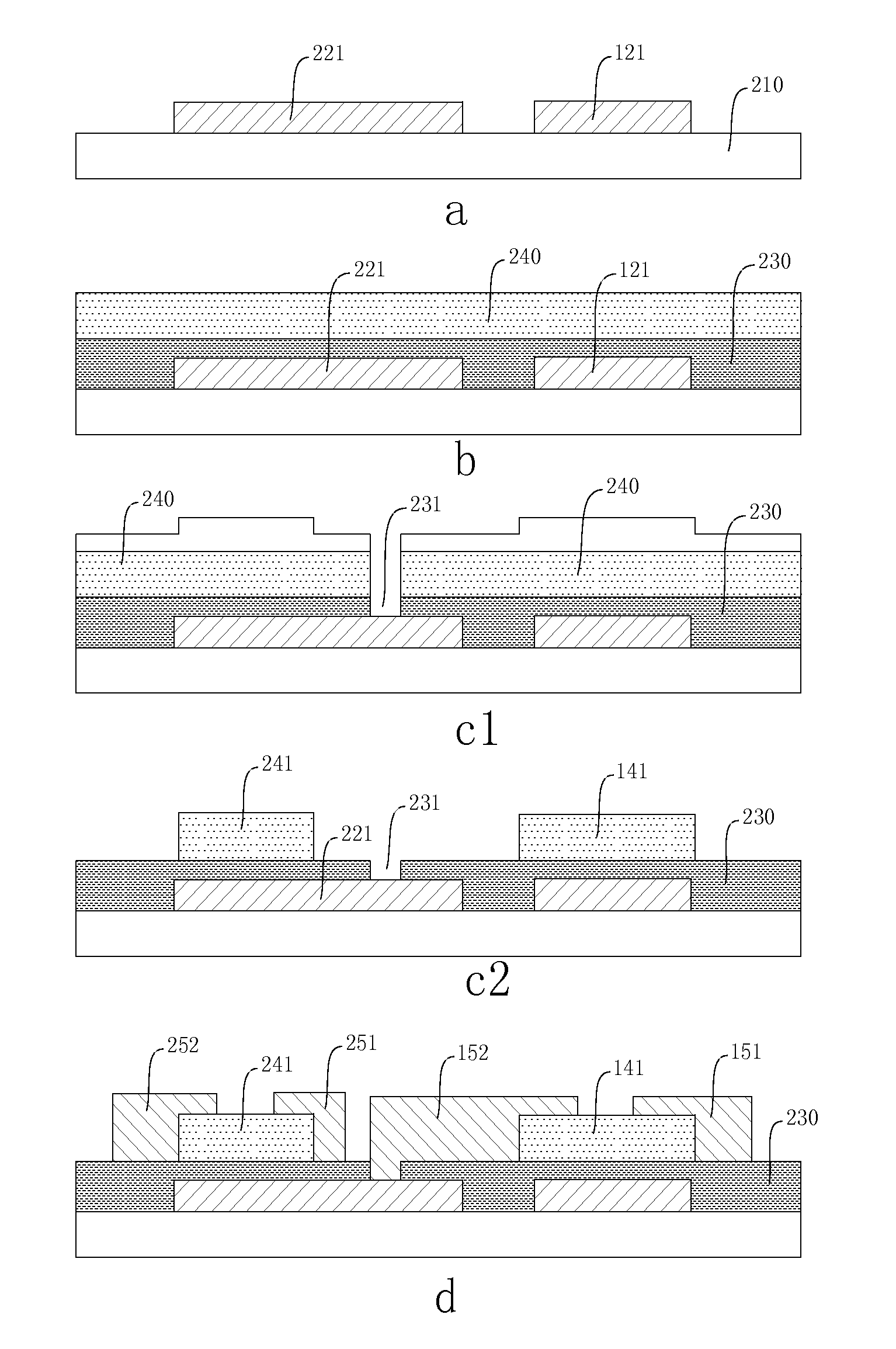
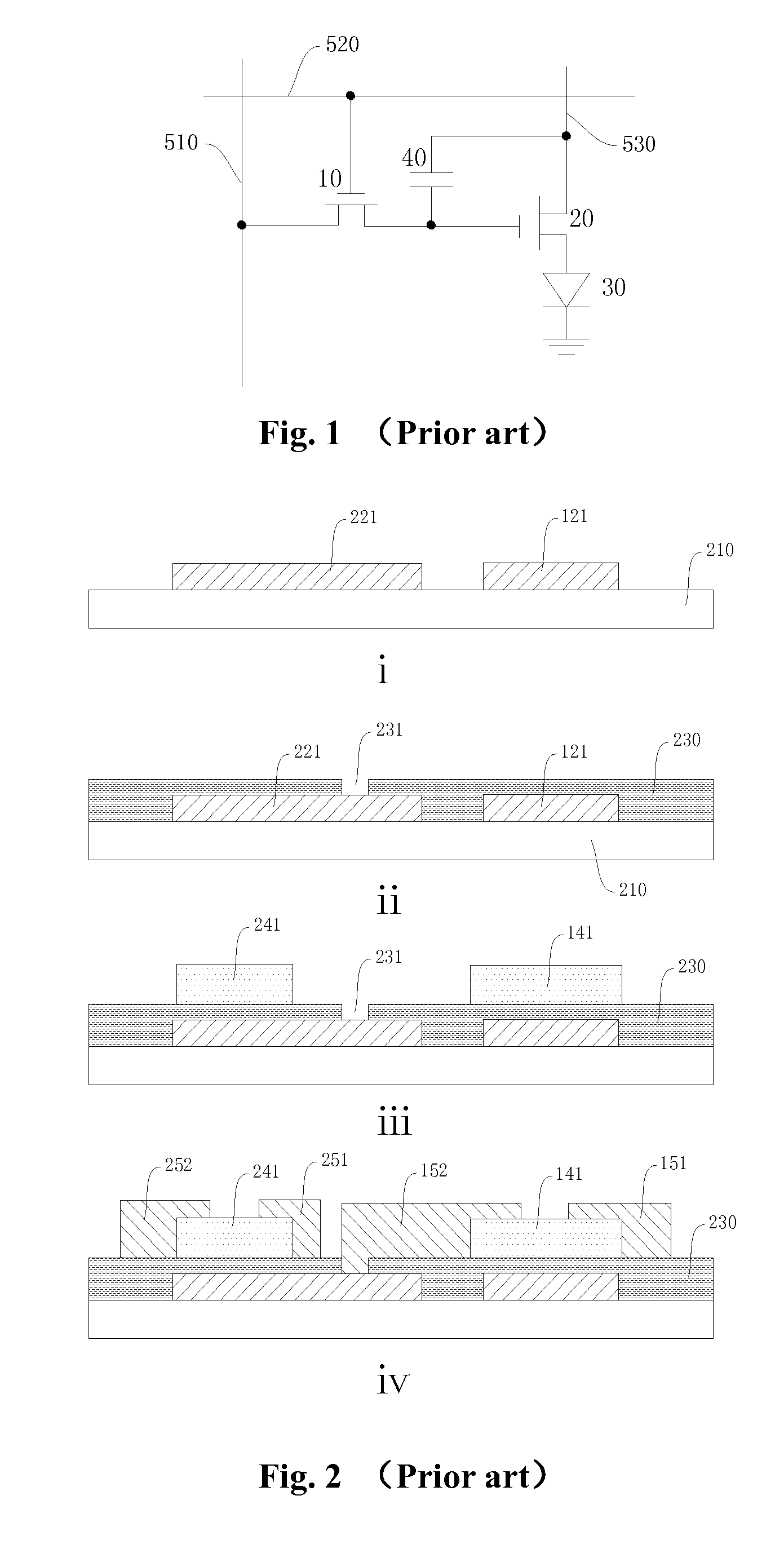
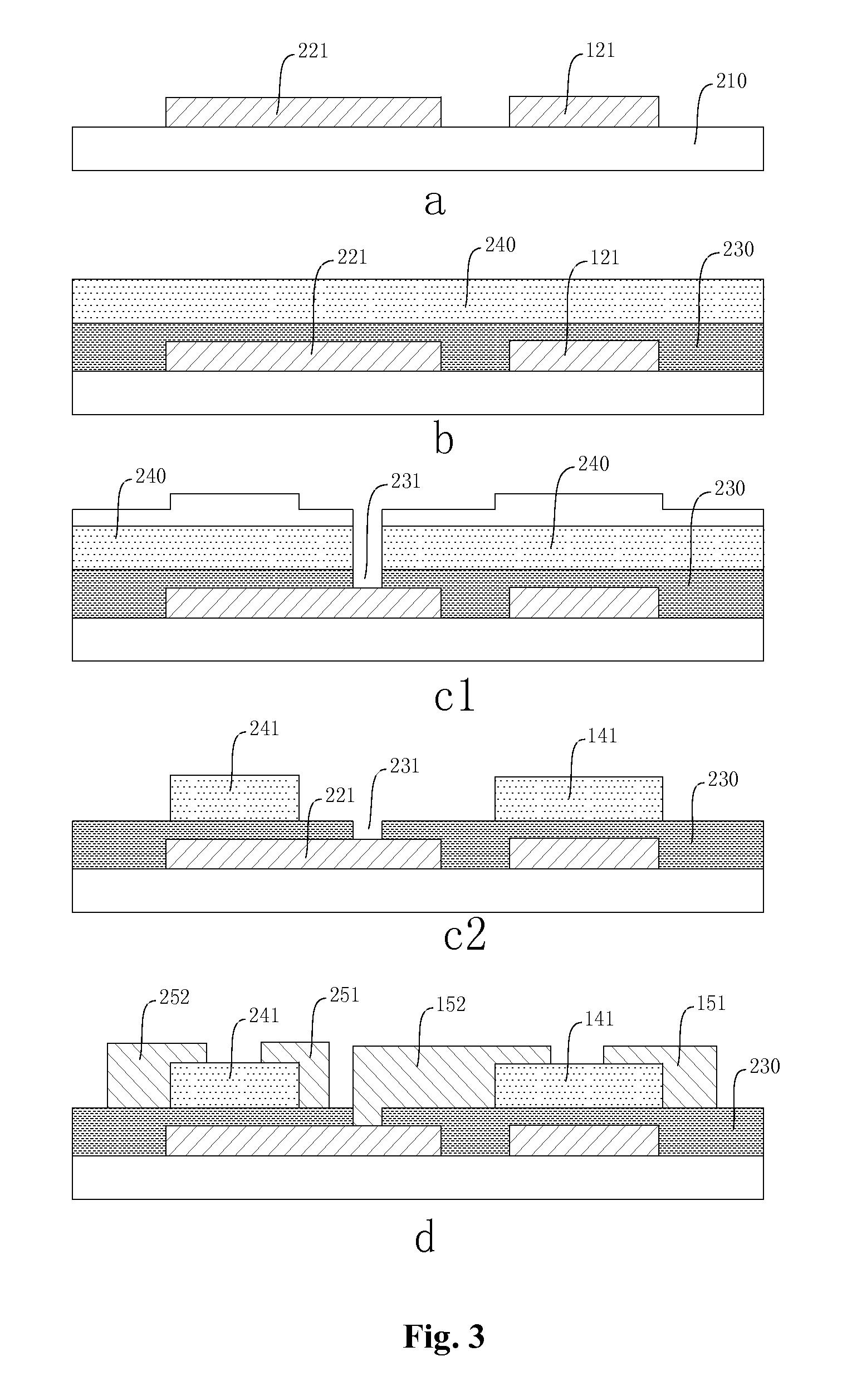
[0036]The present embodiment explains the invention using a pixel region including two thin film transistors and one capacitor having a 2Tr-1Cap structure as illustrated in FIG. 1, wherein the first thin film transistor 10 and the second thin film transistor 20 are both the metal oxide thin film transistors. Or, in other embodiments, the first thin film transistor 10 may also be a polysilicon thin film transistor matched with the second thin film transistor 20. Or, in other embodiments, the method of manufacturing three or more thin film transistors included in the pixel region may also adopt the solution revealed in the present embodiment, wherein the rest thin film transistor and the capacitor are the supplementary circuit for improving the uniformity of the organic light emitting diode 30. The 2Tr-1Cap structure is similar to that of the prior art, which is not explained in more detail here.

[0037]As illustrated in FIG. 3, the first thin film transistor 10 and the second thin film...

embodiment 2

[0046]The present embodiment is different from the embodiment 1 in: the first thin film transistor 10 and the second thin film transistor 20 provided by the present embodiment both have an etch stop layer (ESL) structure. Referring to FIG. 4, the manufacturing method particularly includes:

[0047]a) forming a conductive layer on a substrate 210, depositing a photoresist layer on the conductive layer, and exposing and photoetching the photoresist layer simultaneously, thereby forming a first gate 121 of the first thin film transistor 10 and a second gate 221 of the second thin film transistor 20;

[0048]b) depositing an insulating layer 230 and a semiconductor layer 240 in order above the substrate, wherein the semiconductor layer 240 covers the insulating layer, the insulating layer 230 covers the first gate 121 and the second gate 221. In the present embodiment, the material of the insulating layer 230 is silicon oxide, and the material of the semiconductor layer 240 is IGZO. Of course...


PUM


Abstract

A method of manufacturing transistor having a first and second thin film transistor by creating the second thin film transistor by forming a second gate of the second thin film transistor on a substrate, depositing an insulating layer and a semiconductor layer in order to cover the second gate. A photoresist layer is deposited above the semiconductor layer and exposed. The semiconductor layer and the insulating layer are etched, thereby forming a second active layer of the second thin film transistor and a first connection window disposed above the second gate. A second source and a second drain of the second thin film transistor is deposited above the insulating layer and the second active layer. The present method enables the manufacturing of an organic light emitting diode display. The method reduces the times of using a photomask, thereby saving the manufacture time, improving the productivity and economizing the manufacture cost.

Description

BACKGROUND[0001]1. Technical Field[0002]The present invention relates to a liquid crystal display technical field; more particularly, to a method of manufacturing a thin film transistor and a method of an organic light emitting diode display.[0003]2. Background Art[0004]A flat panel display is widely applied for the advantages, such as thin body, low power consumption, etc., and the existing flat panel display generally includes a liquid crystal display (LCD) and an organic light emitting diode display (OLED).[0005]The organic light emitting diode display is a self-luminous display device that displays an image through an organic light emitting diode. Different from the liquid crystal display (LCD), the organic light emitting diode display emits the light using the energy generated by excitons, which are generated by combining electron-hole in the organic emitting layer, from an excited state to a ground state, which does not need a separate light source accordingly, thereby having ...

Claims


Application Information

Patent Timeline
IPC IPC(8): H01L29/66H01L27/32H01L29/786H01L21/311H01L21/02
CPCH01L29/66969H01L21/31144H01L27/3244H01L29/7869H01L21/0206H10K59/122H10K71/233H10K59/1201H01L21/0274H01L27/1288H01L27/1225H10K59/12
Inventor LV, XIAOWENTSENG, CHIHYUAN
Owner TCL CHINA STAR OPTOELECTRONICS TECH CO LTD
Learn More