Thin film transistor and display device

Active Publication Date: 2015-10-29
NEC LCD TECH CORP +1
View PDF8 Cites 17 Cited by
  • Summary
  • Abstract
  • Description
  • Claims
  • Application Information

AI Technical Summary

Benefits of technology

[0029]The thin film transistor according to an exemplary aspect of the invention is characterized as a thin film transistor which includes: a channel region, an LDD region, and a drain region formed with a polycrystalline silicon active layer; a gate electrode provided at least in the channel region via a gate insulating film; and an electrically floating light-shielding layer which overlaps at least wi

Problems solved by technology

However, the resolution limit in a process of manufacturing such as the minimum line width and the like cannot simply be overcome even when the pixel size is reduced.
However, the polycrystalline silicon TFT when used with the high-luminance backlight directly receives irradiation of 1,000,000 cd/m2 level, for example, so that leakage current under an off state is increased due to carriers generated by photoexcitation.
Therefore, the influences of the light from the backlight to the polycrystalline silicon TFT cause display failures, operation malfunctions, and the like, e.g., deterioration in the contrast and increase in crosstalk, flicker, and the like.
However, the biggest issue of this technique is that the number of steps in the manufacture process is increased so that the cost is increased without questions.
Thus, this technique does not regulate a specific range regarding the geometrical shape of the transistor and the layout of the electrodes.
However, while the leakage current in the gate voltage to be off is extremely small, the current flown between the source and drain in a sub-threshold region having voltage of equal to or less

Method used


Image

  • Thin film transistor and display device
  • Thin film transistor and display device
  • Thin film transistor and display device

Examples


Example

First Exemplary Embodiment

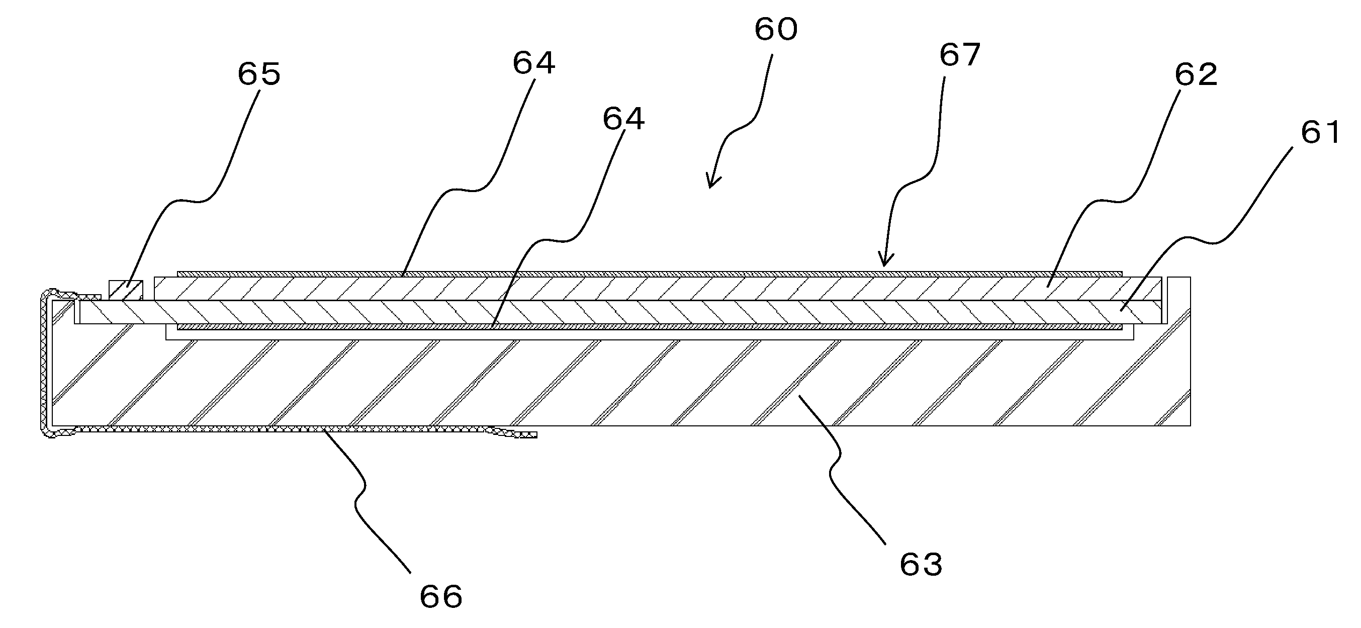
[0087]In a first exemplary embodiment, in order to suppress the characteristic fluctuation of the thin film transistor caused due to the existence of the floating light-shielding layer, i.e., in order to suppress the phenomenon where the threshold voltage changes depending on the drain voltage, the geometrical layout of the light-shielding layer is regulated. Specifically, the film thickness of the underlying insulating layer which determines the distance between the light-shielding layer and the active layer is set to be in a range of 200 nm to 500 nm, both inclusive, and more preferable to be in a range of 300 nm to 400 nm, both inclusive. On that condition, the ratio Sg / Sd (where the opposing area of the drain region of the active layer and the light-shielding layer is defined as Sd, and the opposing area of the gate electrode and the light-shielding layer is defined as Sg) is taken as an indicator expressed as the G / D ratio which is preferable to be set...

Example

Second Exemplary Embodiment

[0171]In the first exemplary embodiment, the method regarding the layout of the light-shielding layer for suppressing the characteristic fluctuation in the dual-gate thin film transistor is described. The result acquired by applying the same idea to a single-gate thin film transistor will be described as a second exemplary embodiment.

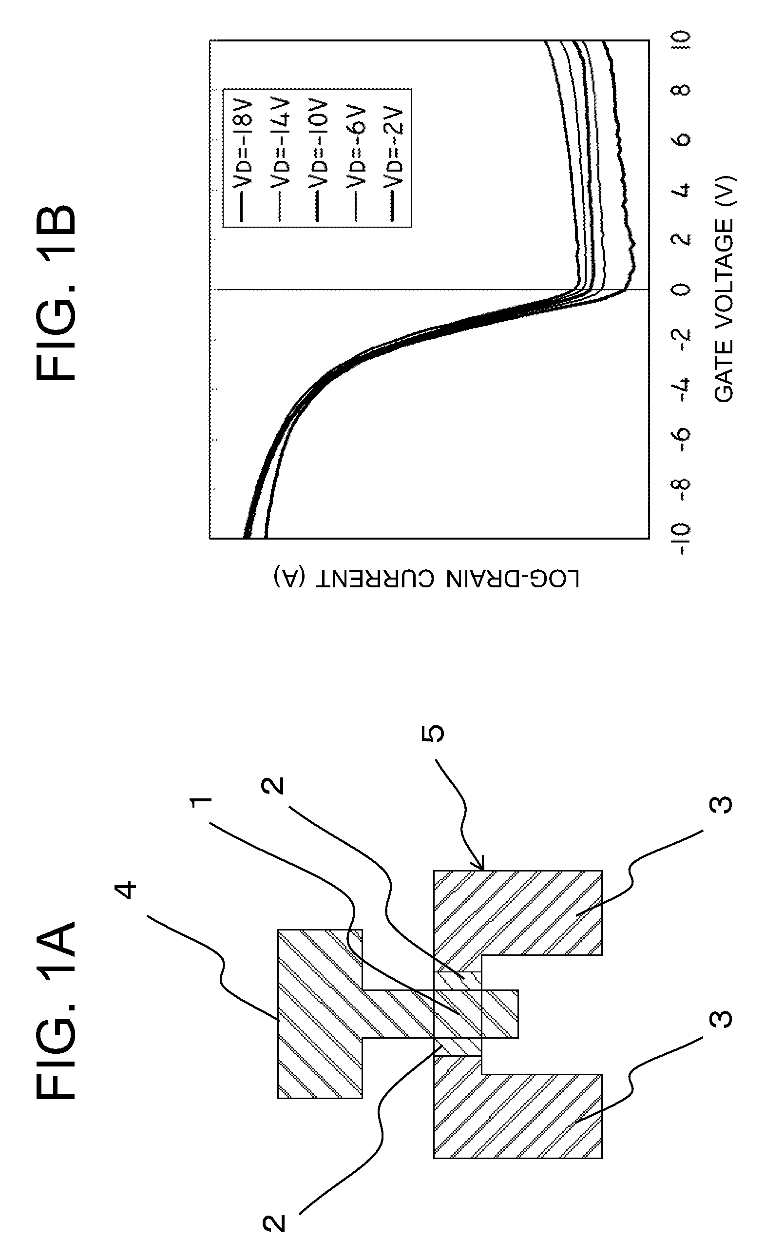
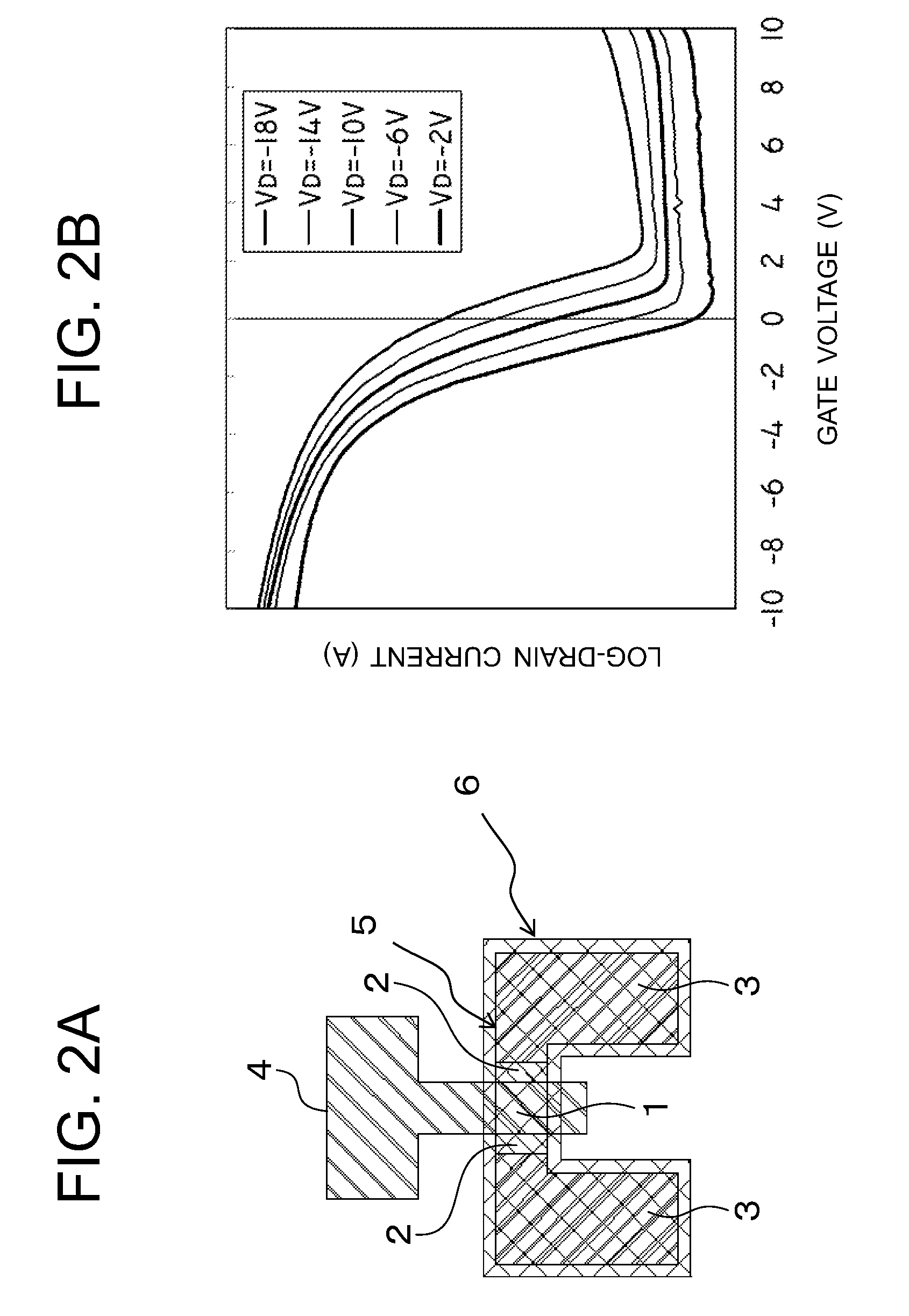
[0172]With the single-gate transistor, the change width dVth of the threshold voltage Vth of the transistor is determined by the ratio G / D=Sg / Sd provided that Sg is the overlapping area of the light-shielding layer and the gate layer and Sd is the overlapping area of the light-shielding layer and the drain layer. The characteristic fluctuation was measured by changing the shape of the light-shielding layer in the transistor of the basic layout as shown in FIG. 1A, and a regression analysis was performed on the acquired data. FIG. 21 shows the result. A regression equation can be written as follows.

dVth=α·ln(Sg / Sd)+β

α=−0.153 / tu...

Example

Third Exemplary Embodiment

[0186]It has been mentioned that there are changes in the threshold voltage Vth depending on Vd as the characteristic fluctuation caused by the floating light-shield layer. Now, a model of a dual-gate transistor in which a drain voltage Vd is applied by taking a source voltage Vs as the reference will be discussed. FIG. 24A is an equivalent circuit when a common light-shielding layer is provided in a dual-gate transistor. Vg, Vd, Vs, and Vm show the potentials at the point shown in the drawing.

[0187]The models of the first and second exemplary embodiments are to suppress the influence of Vd to a prescribed range by adjusting the ratio of the opposing areas based on the model, in which the potential of the light-shielding layer is determined with a balance between the influence of Vd imposed upon the potential of the light-shielding layer through the opposing face Cd between the drain region and the light-shielding layer and the influence of the gate voltage...


PUM


Abstract

For improved high-definition of liquid crystal display devices and the use thereof in bright places, luminance of backlights is being increased. Thus, when a light-shielding layer is employed for suppressing a light leakage current, characteristic fluctuations of transistors are caused, which may result in showing faulty display. In a dual-gate thin film transistor having a floating light-shielding layer, the layout is designed in such a manner that the film thickness of the insulating layer is equal to or more than 200 nm and equal to or less than 500 nm and that Sg/Sd becomes 4.7 or more, provided that an opposing area between the light-shielding layer and a drain region in a place at the outermost side of the active layer is Sd and the opposing area between the light-shielding layer and the gate electrode is Sg.

Description

CROSS-REFERENCE TO RELATED APPLICATION[0001]This application is based upon and claims the benefit of priority from Japanese patent application No. 2014-090724, filed on Apr. 24, 2014, the disclosure of which is incorporated herein in its entirety by reference.BACKGROUND OF THE INVENTION[0002]1. Field of the Invention[0003]The present invention relates to a thin film transistor and a display device which includes the thin film transistor. More specifically, the present invention relates to an active matrix type liquid crystal display device which is a display device that uses a high-luminance light source.[0004]2. Description of the Related Art[0005]Recently, regarding flat panel displays such as liquid crystal displays (LCD), there are more proposals for various forms of apparatuses represented by keywords such as wearable and ubiquitous, more diversifications of use environments, and the like. Accordingly, demands for small and high-definition displays to be loaded in mobile smartp...

Claims


Application Information

Patent Timeline
IPC IPC(8): H01L29/786H01L27/12
CPCH01L27/124H01L29/78675H01L29/78621H01L29/78633H01L29/78645H01L29/78696
Inventor SEKO, NOBUYAHATAZAWA, YOSHIKAZUSEKINE, HIROYUKI
Owner NEC LCD TECH CORP
Why Eureka
Try Eureka