Ranging apparatus, imaging apparatus, ranging method and ranging parameter calculation method
- Summary
- Abstract
- Description
- Claims
- Application Information
AI Technical Summary
Benefits of technology
Problems solved by technology
Method used
Image
Examples
embodiment 1
Ranging Apparatus, Ranging Method
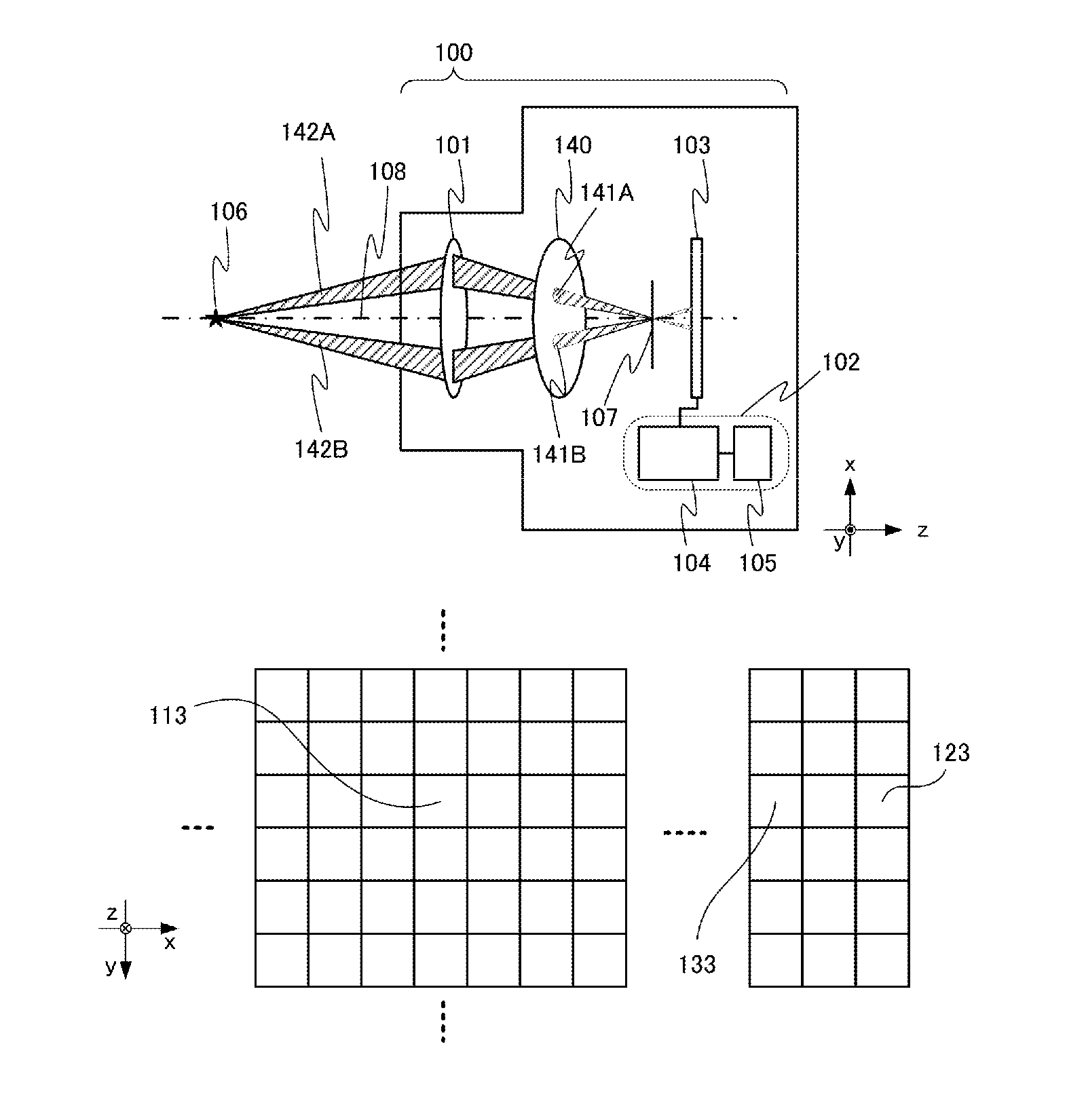
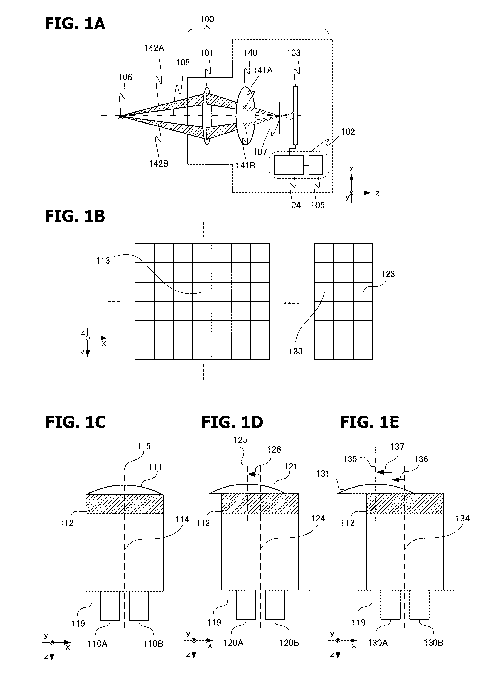
[0025]FIG. 1A is a schematic diagram depicting an imaging apparatus 100 that includes a distance detection apparatus according to this embodiment. The imaging apparatus 100 is constituted by an imaging optical system 101, a distance detection apparatus (ranging apparatus) 102, and an image sensor 103. The distance detection apparatus 102 includes a processing unit 104 and a memory 105. In the following description, the optical axis 108 of the imaging optical system 101 is parallel with the z axis. The x axis and the y axis are perpendicular to each other, and are perpendicular to the optical axis 108.
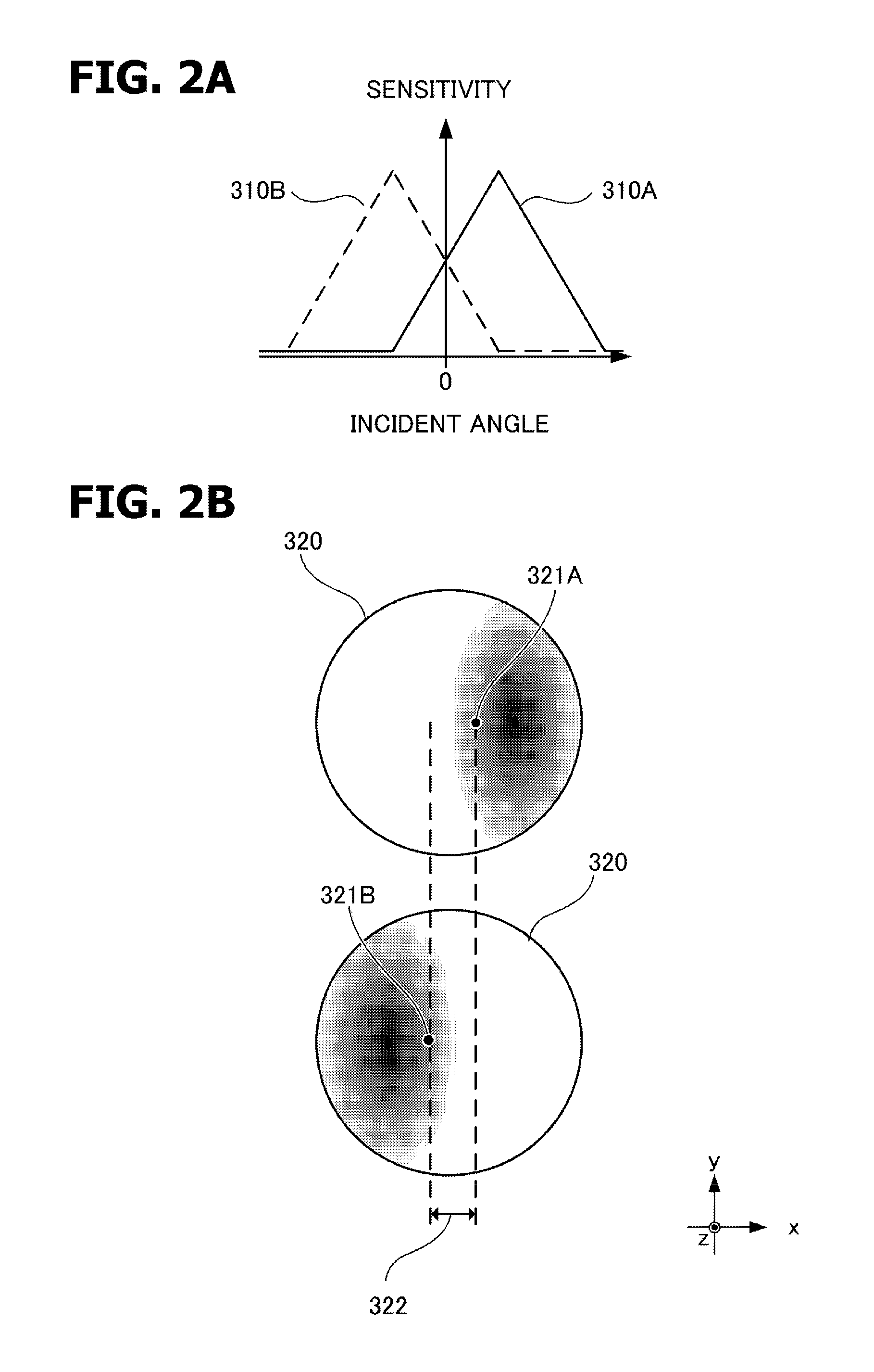
[0026]The image sensor 103 is constituted by many ranging pixels (hereafter also simply called “pixels” for brevity), which are arrayed on the xy plane, as depicted in FIG. 1B. A pixel 113 at the center of the image sensor 103 is constituted by a micro-lens 111, a color filter 112, and photoelectric conversion units 110A and 110B as depicted in the cross...
embodiment 2
[0060]In this embodiment, described will be a base line length correction method for correcting the base line length change due to a fabrication error, which particularly is caused by a parallel shift of the position of the micro-lens array from the design value in the imaging plane all over the surface of the image sensor.
[0061]FIG. 7A is a cross-sectional view when the image sensor 103 is viewed from a direction perpendicular to the z axis which is parallel with the optical axis 108. Each pixel (pixel 901) of the image sensor is constituted by a photoelectric conversion unit 911A (pixel A) and a photoelectric conversion unit 911B (pixel B). A micro-lens array 921 is disposed above the photoelectric conversion units, and the position of the micro-lens array 921 is shifted from the design value by a micro-lens shift amount in accordance with the position of each pixel. The micro-lens array has a micro-lens shift error in the shift direction 931, which is parallel with the +x directi...
embodiment 3
[0063]In this embodiment, described will be a base line length correction method for correcting the base line length change due to a fabrication error, which particularly is caused by a shift (contraction) of the position of the micro-lens array toward the center of the image sensor in the imaging plane all over the surface of the image sensor.
[0064]FIG. 8A is a cross-sectional view when the image sensor 103 is viewed from a direction perpendicular to the z axis, which is parallel with the optical axis of the image sensor 103, just like Embodiment 2. Each pixel (pixel 1001) of the image sensor is also constituted by a photoelectric conversion unit 1011A (pixel A) and a photoelectric conversion unit 1011B (pixel B). A micro-lens array 1021 is disposed above the photoelectric conversion units, and the position of the micro-lens array 1021 is shifted from the design value by a micro-lens shift amount in accordance with the position of each pixel. The micro-lens array has a micro-lens s...
PUM
 Abstract
Description
Claims
Application Information


