Multilayer circuit board and method for manufacturing the same

a multi-layer circuit board and manufacturing method technology, applied in the direction of superimposed coating process, resistive material coating, liquid/solution decomposition chemical coating, etc., can solve the problem of high-power chips generating large amount of heat when working, reducing heat dissipation efficiency, and undesired stress in the circuit board

Active Publication Date: 2015-11-05
TONG HSING ELECTRONICS IND LTD
View PDF4 Cites 22 Cited by
  • Summary
  • Abstract
  • Description
  • Claims
  • Application Information

AI Technical Summary

Benefits of technology

[0006]Therefore, an object of the present invention is to provide a method for manufacturing a multilayer circuit board that can overcome at least one of the aforesaid drawbacks associated with the prior art.

Problems solved by technology

It is known in the art that high power chips may generate large amount of heat when working.
Since the dielectric layer has a relatively low thermal conductivity value of about 0.1-0.5 W / mK and is sandwiched between the copper layer and the base layer, it becomes a thermal barrier for heat transfer from the copper layer to the base layer, which results in a decrease in heat dissipation efficiency.
In order to secure the metal blocks in the through-holes, the metal blocks have a diameter or cross-section that is slightly greater than those of the through-holes, which causes undesired stress in the circuit board.
In addition, since the metal blocks are formed using mechanical machining techniques, control of machining the same may be relatively difficult and a high precision of the metal blocks may be difficult to achieve when the size and the thickness of the metal blocks are small.
Moreover, since the metal blocks are inserted into the through-holes using a pick and place machine, there may arise a precision problem for alignment of the metal blocks with interconnections that are subsequently formed on the circuit board for connecting the metal blocks to the semiconductor chips and / or components, such that misalignment between the metal blocks and the interconnections tend to occur.

Method used


Image

  • Multilayer circuit board and method for manufacturing the same
  • Multilayer circuit board and method for manufacturing the same
  • Multilayer circuit board and method for manufacturing the same

Examples


Embodiment Construction

[0013]The above-mentioned and other technical contents, features, and effects of this invention will be clearly presented from the following detailed description of the embodiment in coordination with the reference drawings.

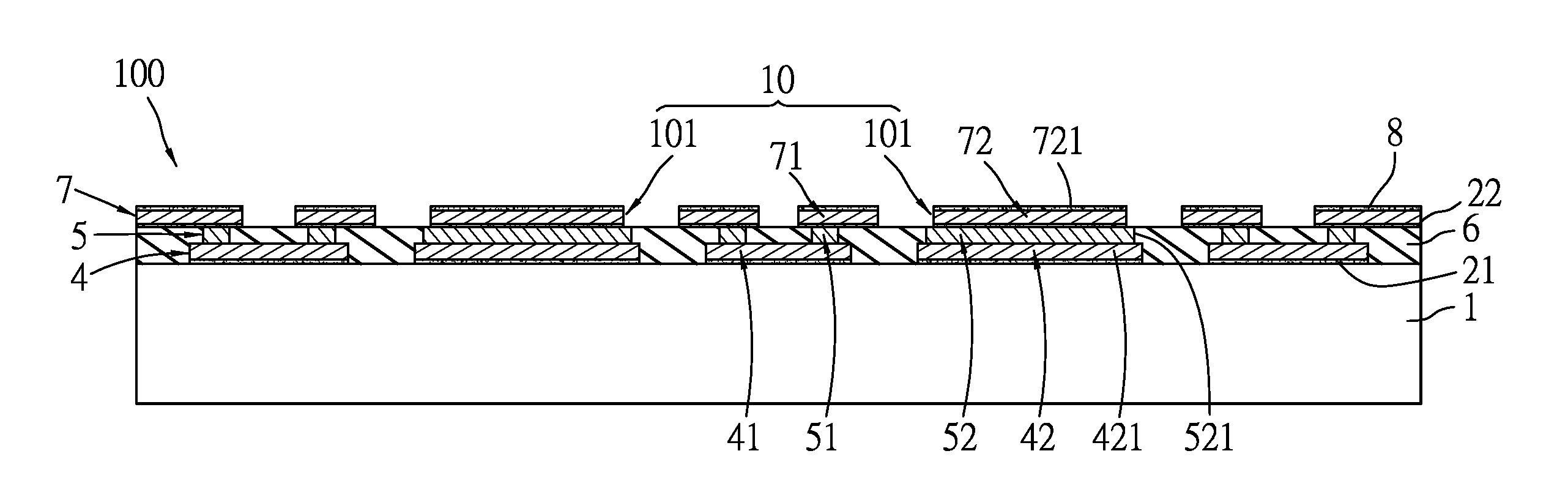
[0014]FIG. 15, together with FIGS. 1 to 14, illustrates consecutive steps (S01-S14) of the embodiment of a method for manufacturing a multilayer circuit board having a metallic submount structure 10 for mounting and heat dissipation of at least one semiconductor chip 9(see FIG. 16), such as an LED chip, according to the present invention.

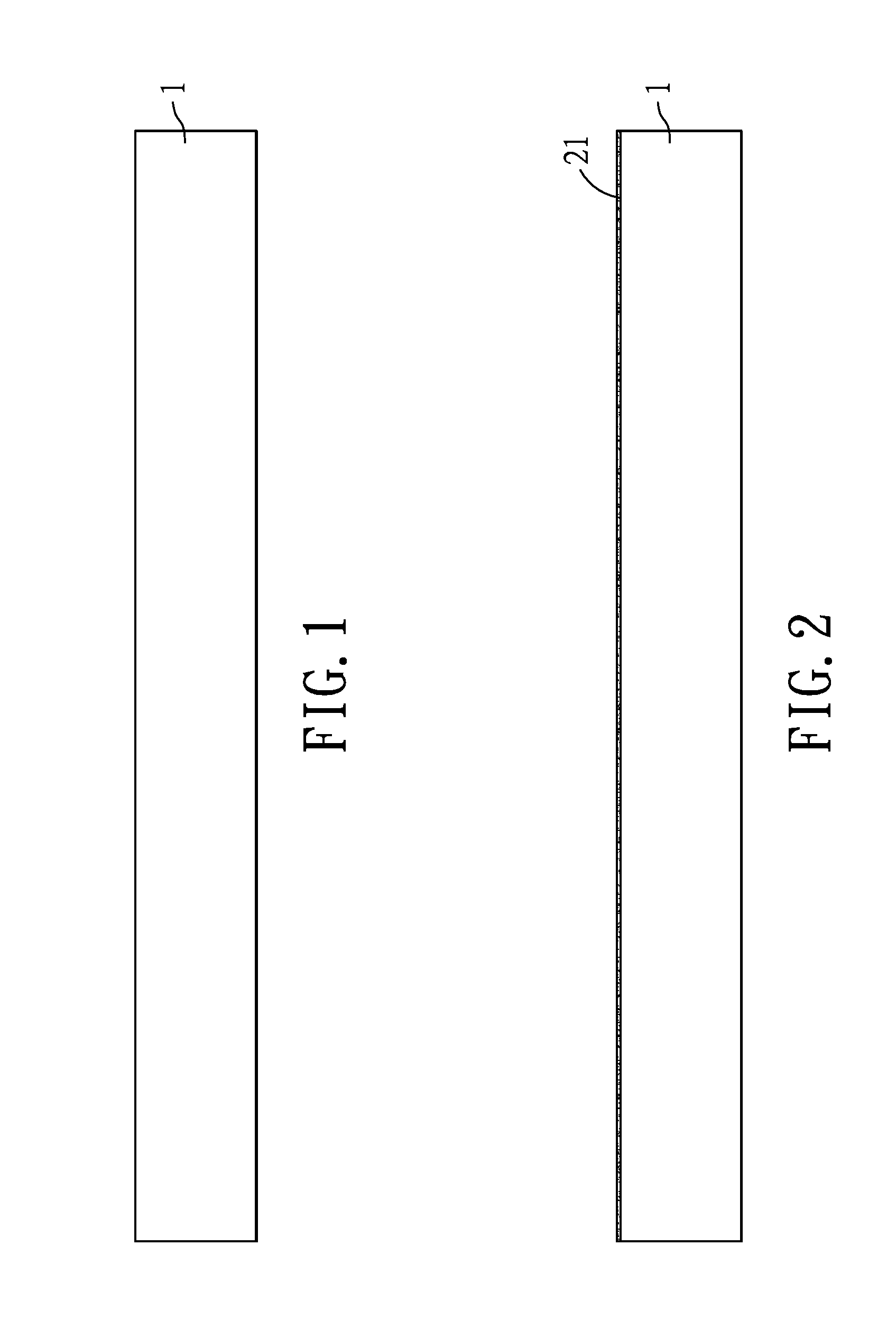
[0015]Step S01: providing a ceramic substrate 1 (see FIG. 1).The ceramic substrate 1 is made from a material selected from the group consisting of aluminum oxide, aluminum nitride, silicon nitride, zirconia, and zirconia toughened alumina.

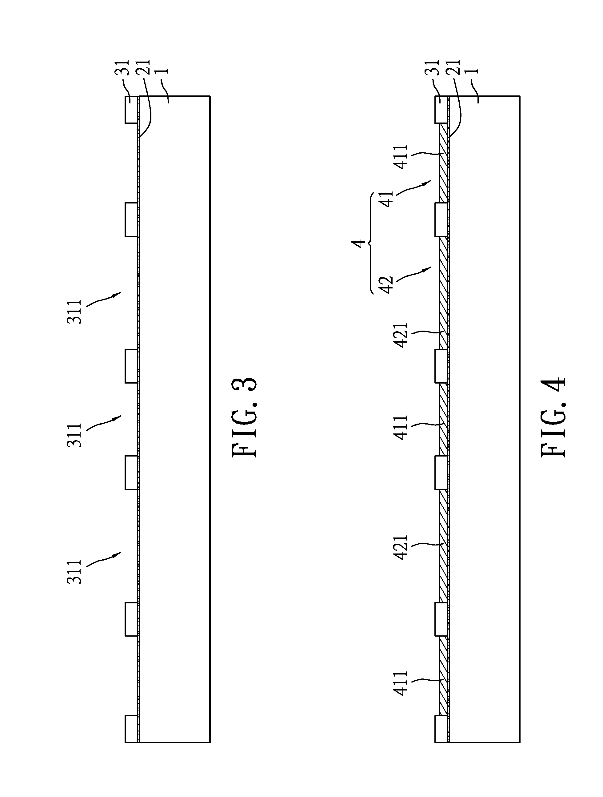
[0016]Step S02: forming a first seed layer 21 on a surface of the ceramic substrate 1 (see FIG. 2) by sputtering. The first seed layer 21 is used for subsequent electroplating.

[0017]Step S03: fo...


PUM

PropertyMeasurementUnit
conductiveaaaaaaaaaa
heataaaaaaaaaa
insulatingaaaaaaaaaa

Abstract

A method for manufacturing a multilayer circuit board includes: forming a first patterned conductive layer on a ceramic substrate, the first patterned conductive layer having a first circuit pattern and a first submount pattern; forming a second patterned conductive layer on the first patterned conductive layer, the second patterned conductive layer having a second circuit pattern and a second submount pattern; forming an insulating layer on the ceramic substrate; and forming a third patterned conductive layer on the insulating layer. The third patterned conductive layer having a third circuit pattern and a third submount pattern. The first, second and third submount patterns are stacked one above another.

Description

CROSS-REFERENCE TO RELATED APPLICATION[0001]This application claims priority of Taiwanese Patent Application No. 103115713, filed on May 1, 2014.BACKGROUND OF THE INVENTION[0002]The invention relates to a multilayer circuit board and a method for manufacturing the same, and more particularly to a method for manufacturing a multilayer circuit board that includes forming a patterned conductive layer which has a submount pattern and a circuit pattern.[0003]It is known in the art that high power chips may generate large amount of heat when working. A circuit board used for mounting the high power chips may be required to have high heat-dissipation efficiency to avoid heat generated from the high power chips from accumulating thereon.[0004]One type of a conventional circuit board, such as Metal Core Printed Circuit Board (MCPCB), has been widely used for mounting the high power chips, especially for mounting LED chips, so that the heat resulting from the high power chips can be efficient...

Claims


Application Information

Patent Timeline
Patent Type & Authority Applications(United States)
IPC IPC(8): H05K3/46H05K3/00H05K1/02H05K1/03H05K1/09
CPCH05K3/46H05K1/0306H05K3/0091H05K1/0298H05K1/092H05K3/4661H05K3/244H05K3/4605H05K2201/10106
Inventor WEI, CHIEN-CHENGCHIANG, TA-HSIANG
Owner TONG HSING ELECTRONICS IND LTD
Why Eureka
Try Eureka