Film forming method, film forming apparatus and recording medium
- Summary
- Abstract
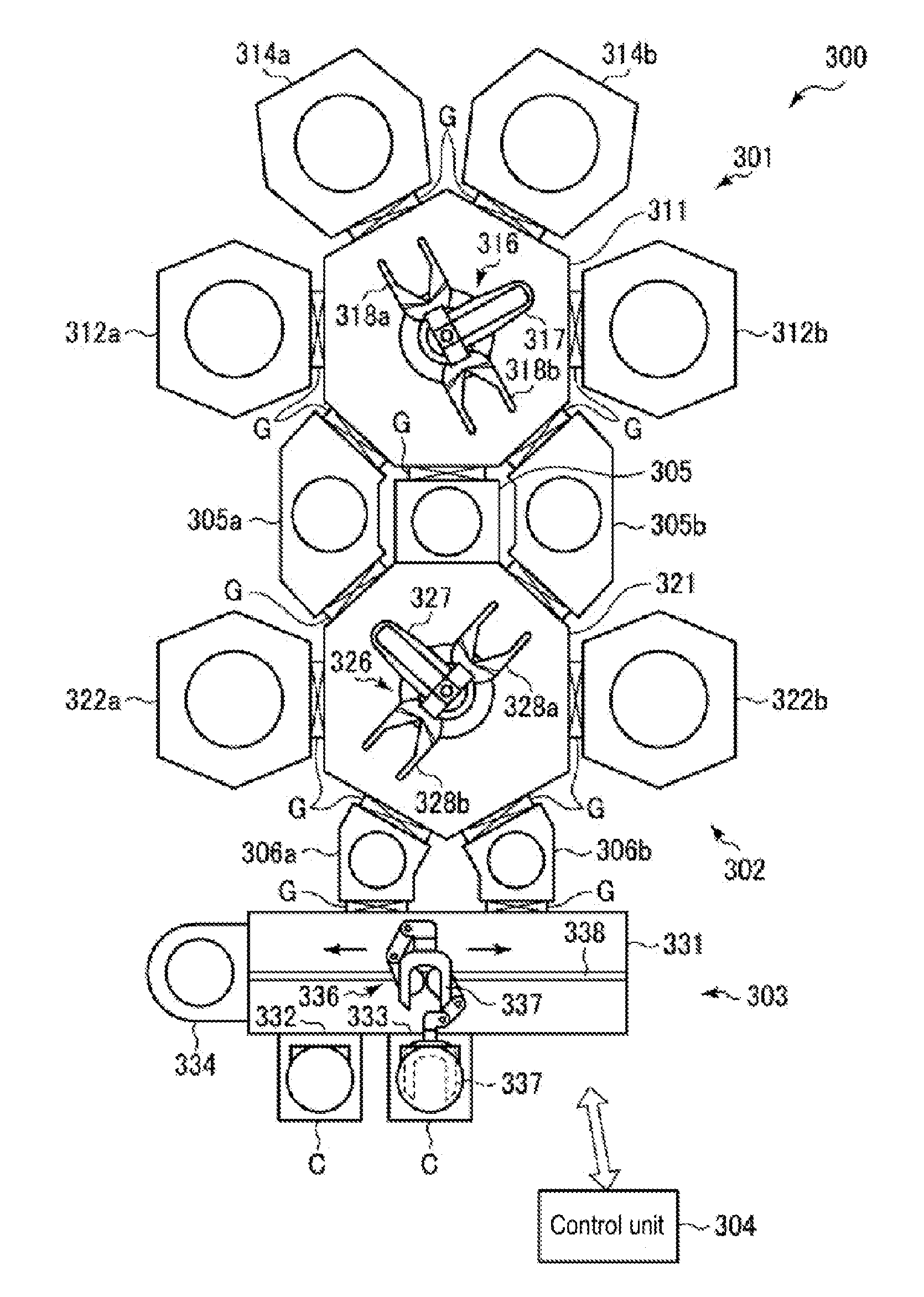
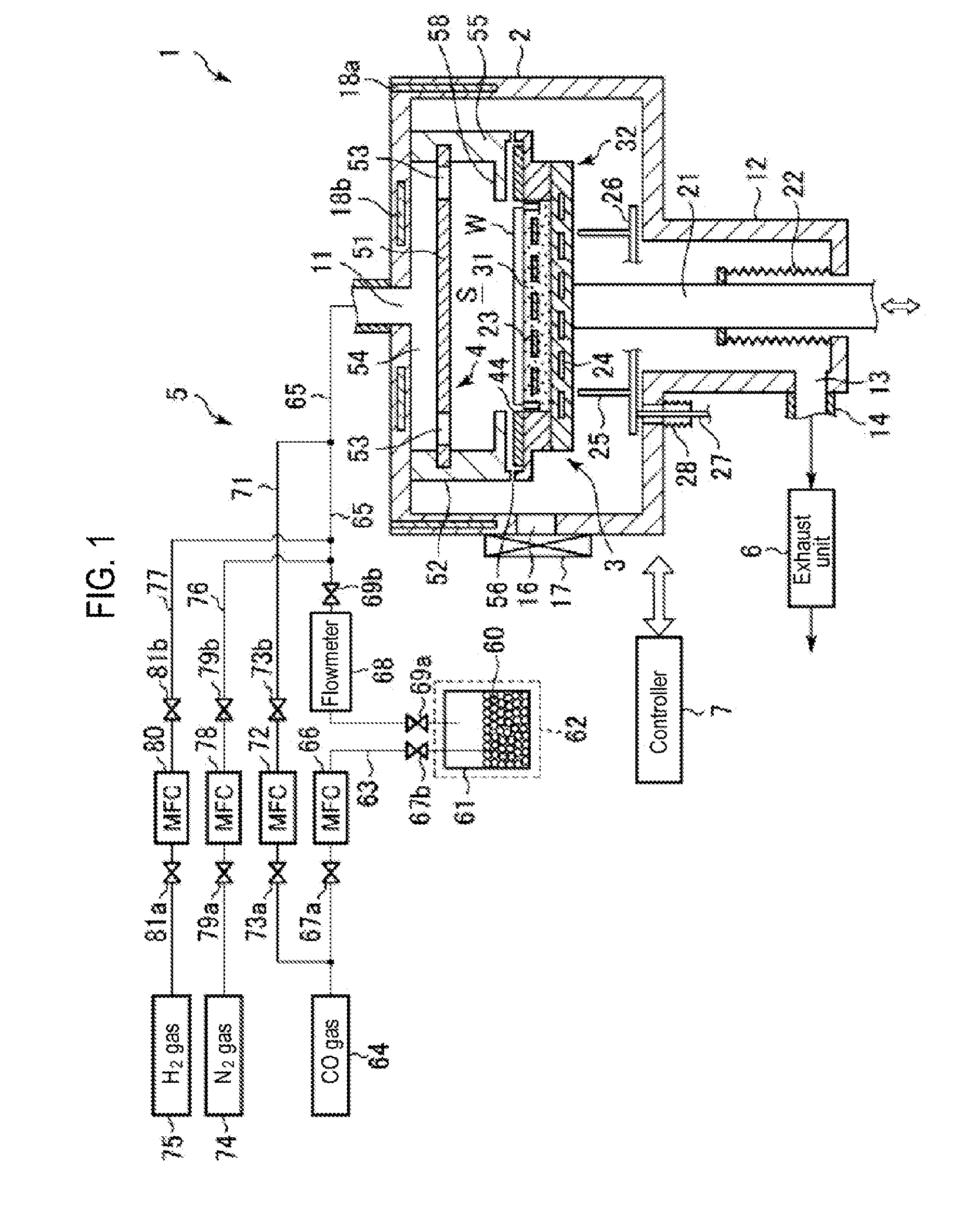
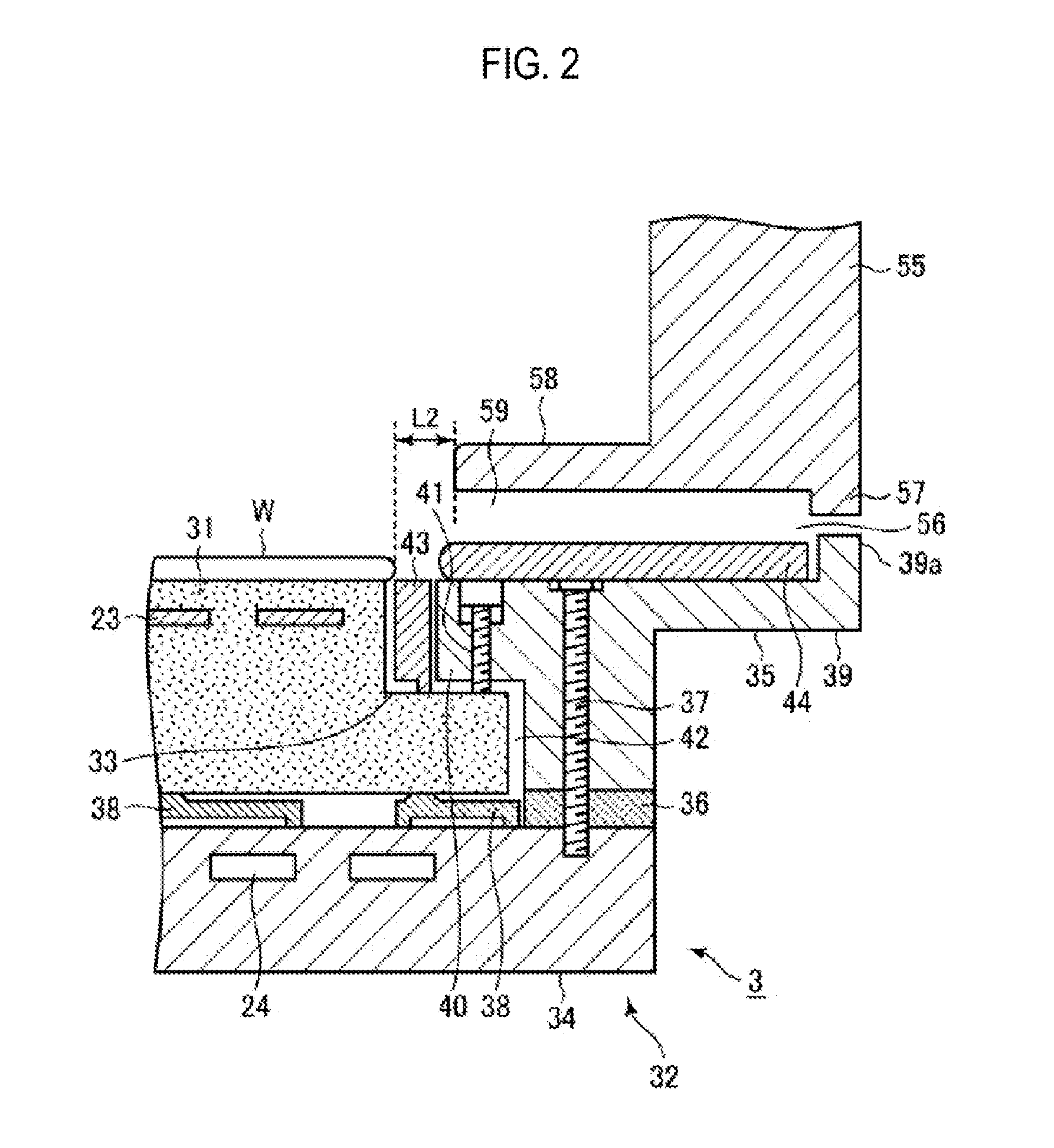
- Description
- Claims
- Application Information
AI Technical Summary
Benefits of technology
Problems solved by technology
Method used
Image

Examples
experimental example
[0081]First, film thicknesses of the Ru films obtained by the method of the present disclosure in which pre-heating is performed with the H2 gas and the method in which pre-heating is not performed were inspected. Here, by using a silicon wafer having a TaN film and a thermal oxide film as a barrier film on an interlayer insulating film formed by ionized physical vapor deposition (iPVD), Ru films having various film thicknesses were formed through CVD in both a case in which pre-heating was performed with the H2 gas and a case in which pre-heating was not performed, and the film thicknesses were measured in a diameter direction of the wafer. FIG. 6 shows film thickness variations (1G) in the diameter direction of the wafer. FIG. 6 also shows the results of lengthening a temperature increasing time with the N2 gas from the conventional 60 sec to 180 sec, without performing pre-heating with the H2 gas, in order to confirm the effect of pre-heating with the H2 gas. As illustrated in FI...
PUM
| Property | Measurement | Unit |
|---|---|---|
| Temperature | aaaaa | aaaaa |
Abstract
Description
Claims
Application Information