Apparatus and method of applying small-angle electron scattering to characterize nanostructures on opaque substrate

Active Publication Date: 2015-11-26
IND TECH RES INST
View PDF5 Cites 6 Cited by
  • Summary
  • Abstract
  • Description
  • Claims
  • Application Information

AI Technical Summary

Benefits of technology

[0014]According to some embodiments, a novel apparatus for small-angle electron scattering in reflection/backscattering modes is provided. This apparatus includes an electron source, a number of electron collimation optics before the sample, a number of electron projection optics after the sample, a sample stage capable of aligning and holding a sample of 40 cm diameter or larger, and a detector module. The electrons emitted from the source are collimated and positioned to impinge on a small target nano-patterned area on an opaque substrate. The signals resulting from the interactions between the impinging electrons and the nanostructures are further magnified by the electron projection optics to reach a sufficient angular resolution before recorded by the detector module.
[0015]According to some embodiments, a novel method of small-angle electron scattering in reflection mode is provided. An electron source is configured to emit electrons. These electrons are reflected/scattered by a target nano-patterned area on an opaque substrate; these reflected/scattered electrons are further magnified by a set of electron projection optics to reach a sufficient angular resolution before recorded by an electron detector module.
[0016]According to some embodiments, a novel method for small-angle electron scattering in backscattering mode is provided. An electron source is configured to emit electrons. After impinging the sample these electrons are backscattered which are further scattered by the target nanostructure located on an opaque substrate, these backscattered then scattered electrons are further magnified by a set of electron projection optics to gain a sufficient angular resolution before recorded by an electron detector module.
[0017]The difference between the present invention and the conventional RHEED/REM includes the apparatus and methods of the above embodiments being capable of measuring or characterizing nano-structure formed on an opaque or thick substrate. Specif

Problems solved by technology

However, it is not feasible to use the conventional RHEED technique to resolve the small-angle scattering signals to reach a sufficient angular resolution in characterizing structures on a nanometer scale.
Synchrotron X-ray sources have often been used for tSAXS measurement and this approach is not amendable to the use in testing laboratories or fabrication lines in semiconductor industries.
Current laboratory X-ray sources can provide app

Method used


Image

  • Apparatus and method of applying small-angle electron scattering to characterize nanostructures on opaque substrate
  • Apparatus and method of applying small-angle electron scattering to characterize nanostructures on opaque substrate
  • Apparatus and method of applying small-angle electron scattering to characterize nanostructures on opaque substrate

Examples


Embodiment Construction

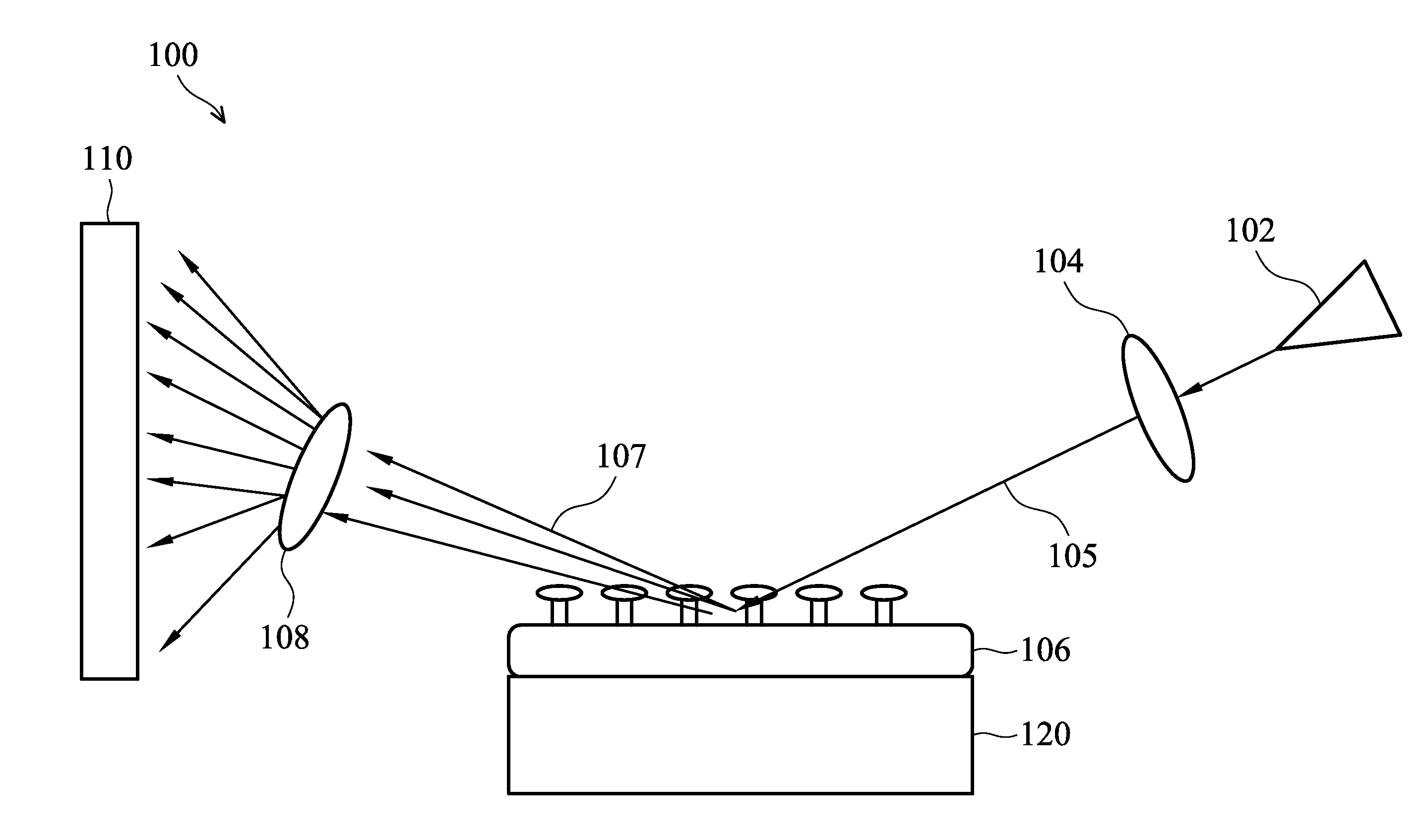
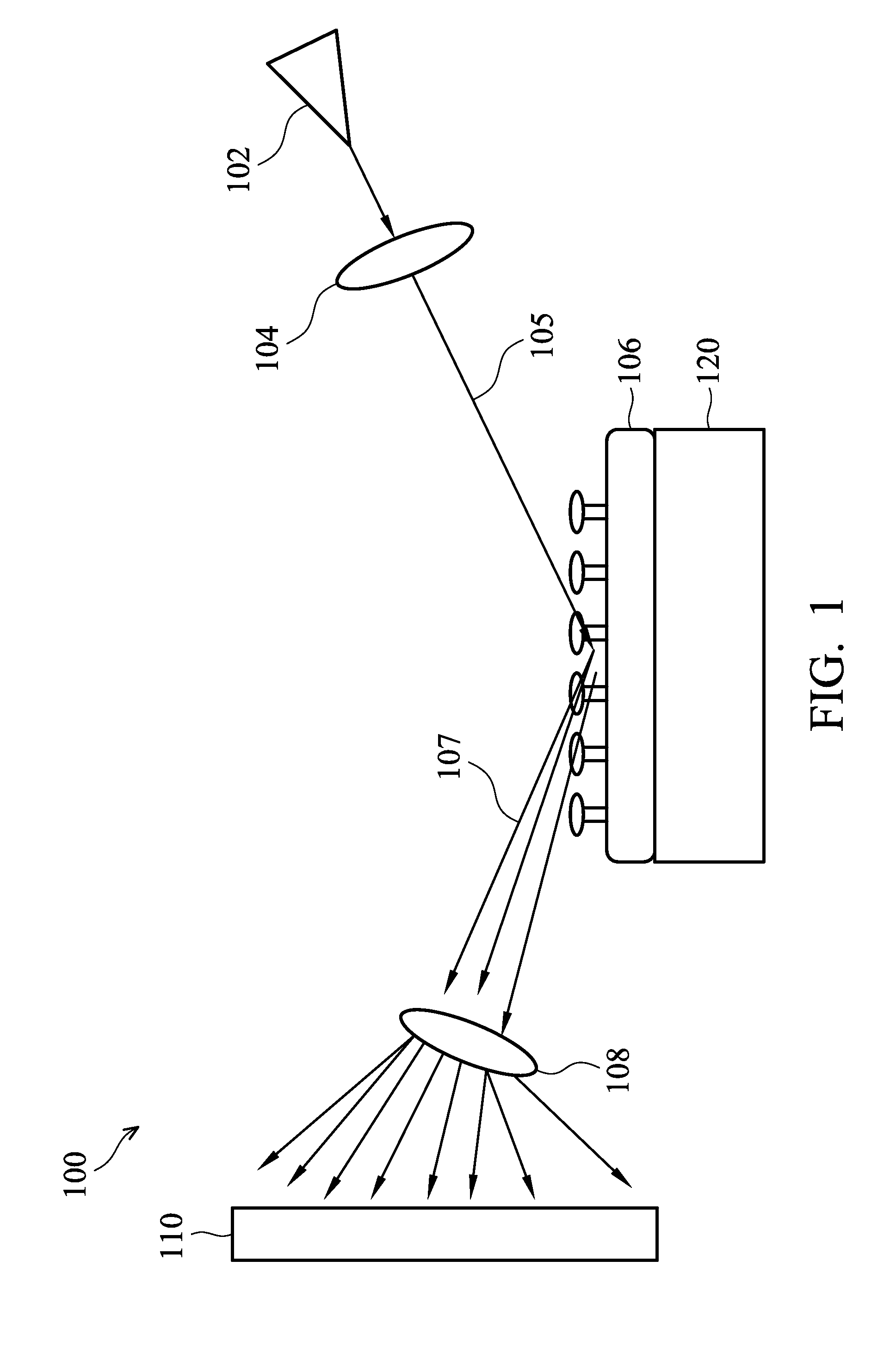
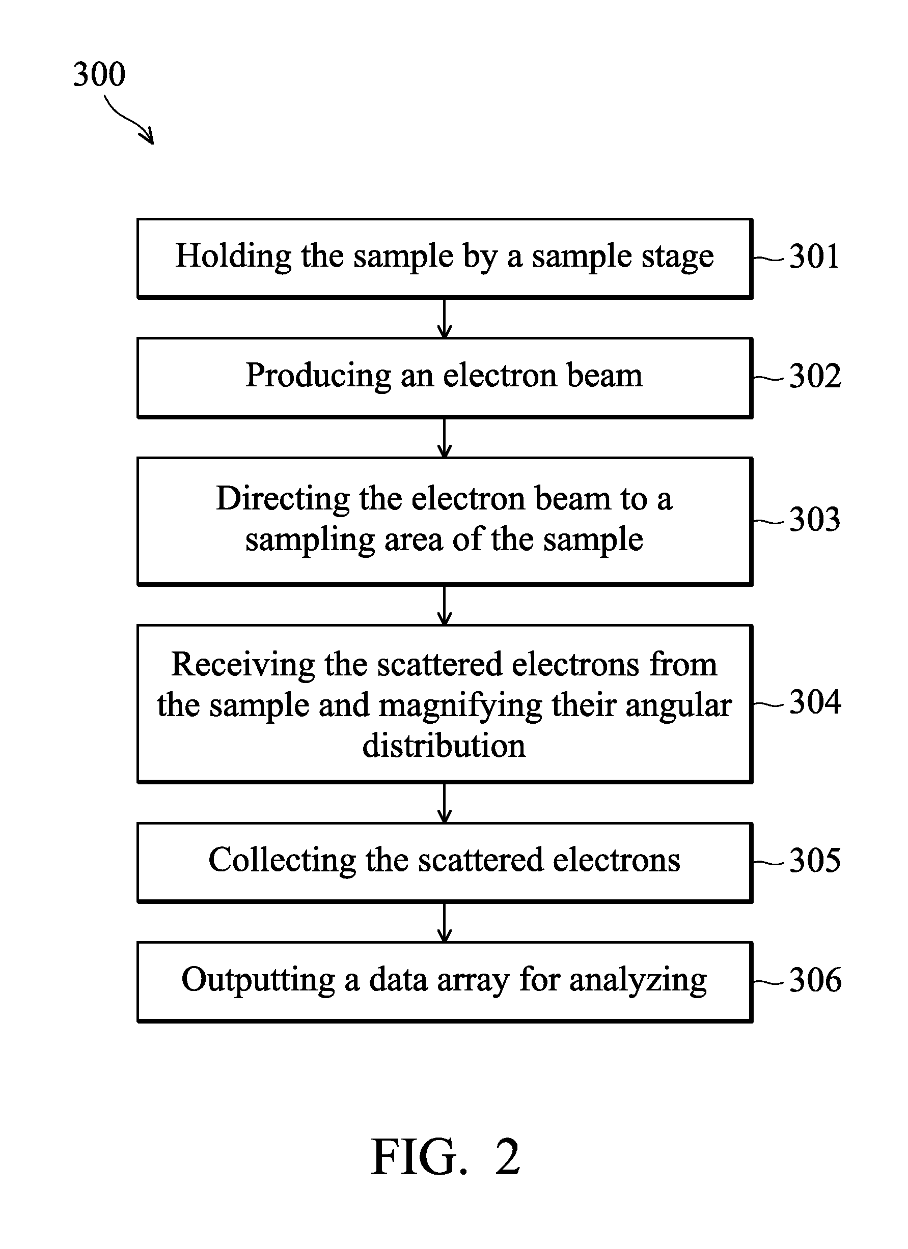
[0026]In the following descriptions, an apparatus and method of applying small-angle electron scattering to characterize nanostructures on opaque substrate of the present invention will be explained with reference to embodiments thereof. It should be appreciated that these embodiments are not intended to limit the present invention to any specific environment, applications or particular implementations described in these embodiments. Therefore, the description of these embodiments is only for the purpose of illustration rather than to limit the present invention. Furthermore, the attached drawings may be drawn in a slightly simplified or exaggerated way for ease of understanding; the numbers, shapes and dimensional scales of elements depicted may not be exactly the same as those in practical implementations and are not intended to limit the present invention.

[0027]In this patent invention a novel electron beam (e-beam) apparatus and methods capable of characterizing nanostructures o...


PUM


Abstract

An apparatus and methods for small-angle electron beam scattering measurements in a reflection or a backscattering mode are provided. The apparatus includes an electron source, electron collimation optics before a sample, electron projection optics after the sample, a sample stage capable of holding the sample, and a electron detector module. The electrons emitted from the source are collimated and positioned to impinge nanostructures on the sample. The signals resulting from the interactions between the impinging electrons and the nanostructures are further magnified by the electron projection optics to reach a sufficient angular resolution before recorded by the electron detector module.

Description

CROSS REFERENCE TO RELATED APPLICATIONS[0001]This application claims the benefit of U.S. Provisional Application No. 62 / 002,537, filed on May 23, 2014, hereby incorporated by reference in its entirety.BACKGROUND[0002]1. Field of the Invention[0003]The present invention relates generally to the characterization of nanostructures on opaque or thick substrates. More particularly, the present invention relates to electron beam metrology in both reflection and backscattering modes applicable to the large sample sizes encountered in today's semiconductor fabrication environments.[0004]2. Description of the Related Art[0005]Reflection high-energy electron diffraction (RHEED) is a powerful analytical tool widely used for characterizing thin film growth in molecular beam epitaxy. It provides great sensitivity in measuring the atomic arrangements, which are in sub-nanometers, of a surface layer by monitoring the electron diffraction patterns; it also has been applied to measuring surface morp...

Claims


Application Information

Patent Timeline
IPC IPC(8): H01J37/29H01J37/147H01J37/145H01J37/06
CPCH01J37/29H01J37/06H01J37/1471H01J37/145H01J2237/2602H01J2237/063H01J2237/04926H01J2237/2007H01J2237/10G01N23/20058H01J37/04H01J37/295H01J2237/0492H01J2237/255
Inventor WU, WEN-LICHIEN, YUN-SANFU, WEI-ENCHEN, YEN-SONGHO, HSIN-CHIA
Owner IND TECH RES INST
Why Eureka
Try Eureka