
Lens array substrate, method of manufacturing lens array substrate, electro-optical device, and electronic apparatus

Inactive Publication Date: 2015-12-10
SEIKO EPSON CORP
View PDF1 Cites 12 Cited by
  • Summary
  • Abstract
  • Description
  • Claims
  • Application Information

AI Technical Summary

Benefits of technology

This patent describes a lens array substrate used in electro-optical devices, such as displays, that improves light utilization efficiency by reducing reflection from the interface between layers having different refractive indexes. This is achieved by sequentially exposing the substrate surface to the lens layer, with fewer layers present at the end of the lens as compared to the central portion. The flattening of the lens layer surface also helps to reduce the number of processes required for manufacturing the lens layer. Overall, this patent provides a solution for improving the display quality and contrast of electronic devices.

Problems solved by technology

For this reason, there is a problem in that the contrast of the liquid crystal device is decreased.
In addition, since an optical path length of the microlens is adjusted by the layer thickness of the uppermost layer of the lens layer, a predetermined layer thickness (residual thickness) has to be secured while flattening the surface in a process of polishing the uppermost layer of the lens layer, and thus there is a problem in that the optical path length cannot be easily adjusted.

Method used


Image

  • Lens array substrate, method of manufacturing lens array substrate, electro-optical device, and electronic apparatus
  • Lens array substrate, method of manufacturing lens array substrate, electro-optical device, and electronic apparatus
  • Lens array substrate, method of manufacturing lens array substrate, electro-optical device, and electronic apparatus

Examples


first embodiment

Electro-Optical Device

[0047]Here, a description will be given by taking an example of an active matrix type liquid crystal device, including a thin film transistor (TFT) as a switching element of a pixel, as an electro-optical device. For example, the liquid crystal device can be preferably used as a liquid crystal light valve of a projector to be described later.

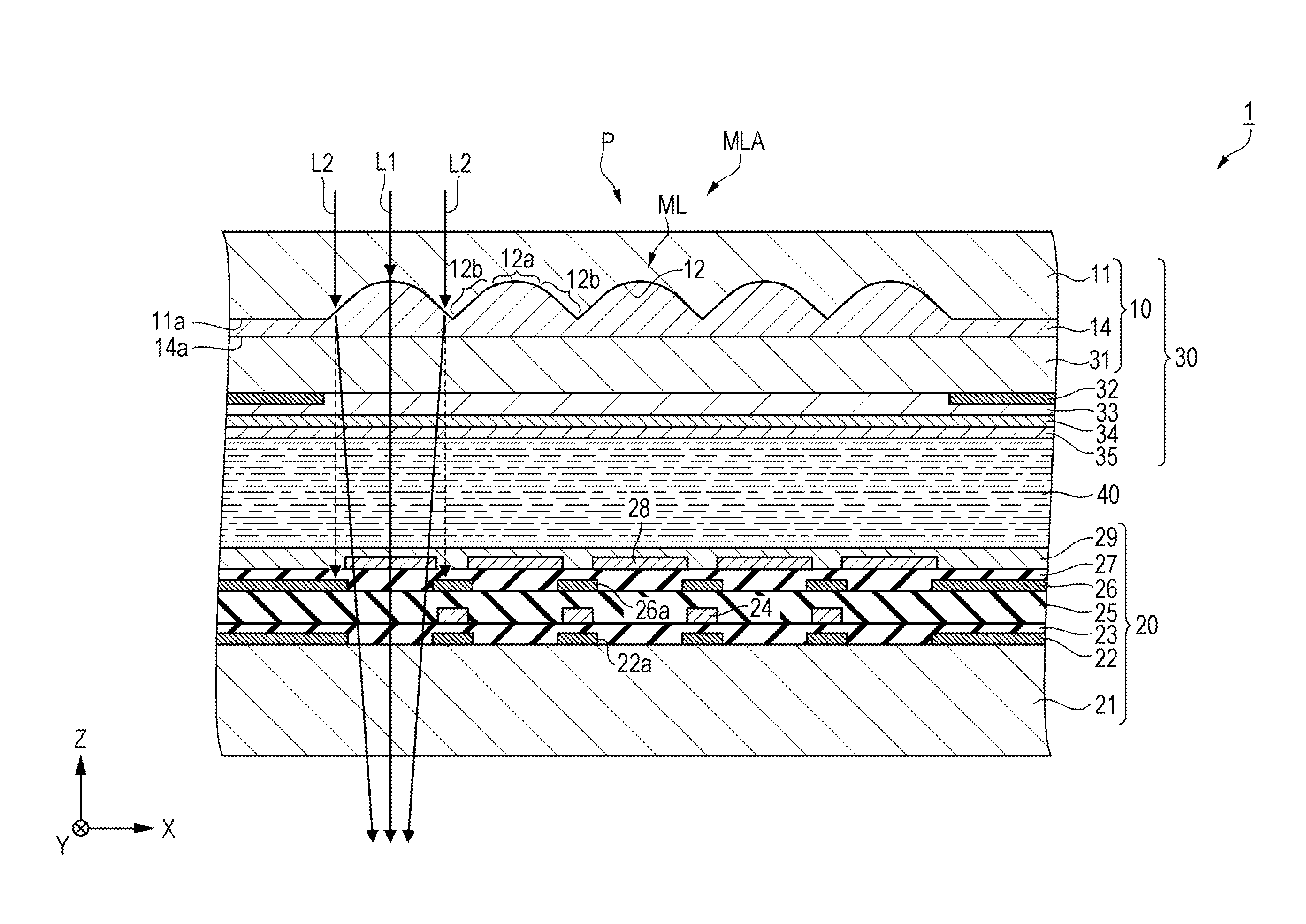
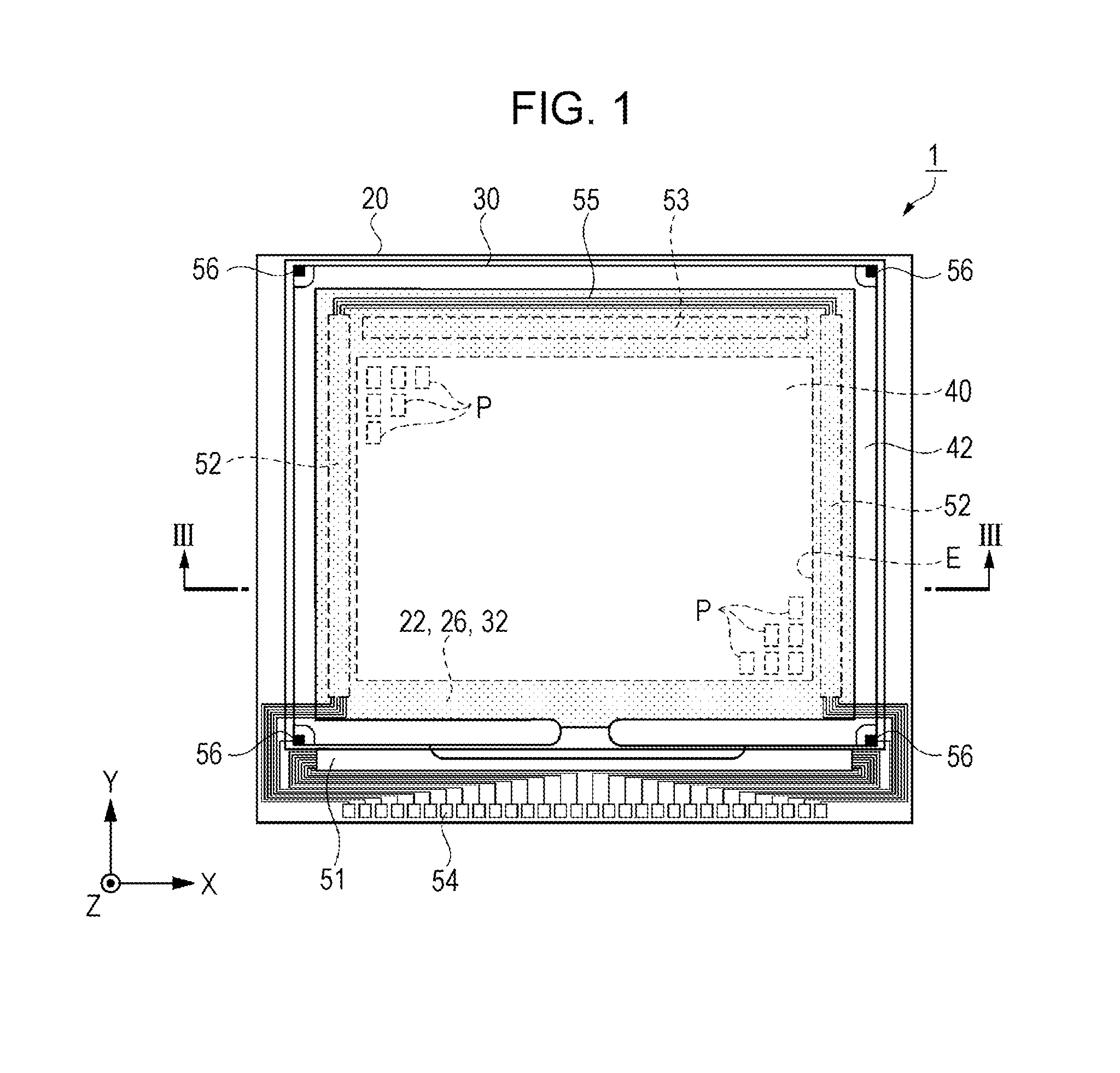
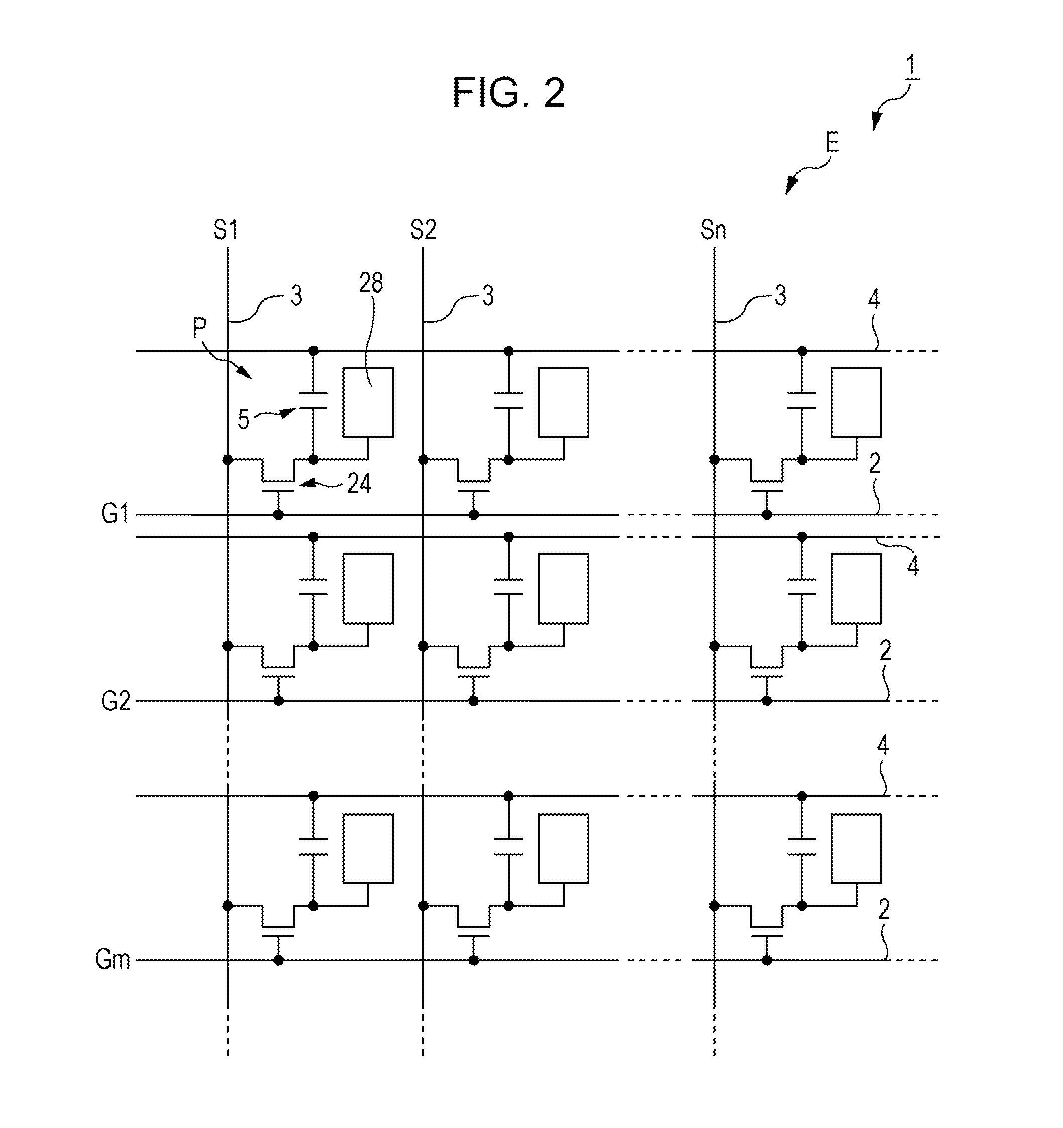
[0048]First, a liquid crystal device as an electro-optical device according to a first embodiment will be described with reference to FIGS. 1 to 3. FIG. 1 is a schematic plan view illustrating the configuration of the liquid crystal device according to the first embodiment. FIG. 2 is an equivalent circuit diagram illustrating an electrical configuration of the liquid crystal device according to the first embodiment. FIG. 3 is a schematic cross-sectional view illustrating the configuration of the liquid crystal device according to the first embodiment. In detail, FIG. 3 is a schematic cross-sectional view taken along line II...

second embodiment

Microlens Array Substrate

[0128]A microlens array substrate according to a second embodiment is different from that in the first embodiment in terms of the configuration of a lens layer. The configuration of a microlens array substrate 10A according to the second embodiment will be described below with reference to FIGS. 8 and 9. FIG. 8 is a schematic plan view illustrating the configuration of the microlens array substrate according to the second embodiment. FIG. 9 is a schematic cross-sectional view illustrating the configuration of the microlens array substrate according to the second embodiment. In detail, FIG. 9 is a schematic cross-sectional view taken along line IX-IX of FIG. 8. Components in common with those in the first embodiment are denoted by the same reference numerals, and the description thereof will be omitted here.

[0129]As illustrated in FIG. 9, the microlens array substrate 10A according to the second embodiment includes a substrate 11 provided with a concave porti...

third embodiment

Electronic Apparatus

[0140]Next, an electronic apparatus according to a third embodiment will be described with reference to FIG. 10. FIG. 10 is a schematic diagram illustrating the configuration of a projector as an electronic apparatus according to the third embodiment.

[0141]As illustrated in FIG. 10, a projector (projection type display device) 100 as an electronic apparatus according to the third embodiment includes a polarized illumination device 110, two dichroic mirrors 104 and 105, three reflecting mirrors 106, 107, and 108, five relay lenses 111, 112, 113, 114, and 115, three liquid crystal light valves 121, 122, and 123, a cross dichroic prism 116, and a projection lens 117.

[0142]The polarized illumination device 110 includes a lamp unit 101 as a light source constituted by a white light source such as, for example, an ultra-high pressure mercury lamp or a halogen lamp, an integrator lens 102, and a polarization conversion element 103. The lamp unit 101, the integrator lens...


PUM


Abstract

A lens array substrate includes a substrate provided with a plurality of concave portions in a first face thereof. The lens layer includes a first lens layer, a second lens layer, and a third lens layer which are sequentially laminated from a substrate side by reflecting the shape of the concave portion therein. A refractive index of the first lens layer is larger than a refractive index of the second lens layer, and a refractive index of the third lens layer is smaller than the refractive index of the second lens layer and is larger than a refractive index of the substrate. The third lens layer, the second lens layer, and the first lens layer are sequentially exposed to the surface of the lens layer toward the end from the central portion of the concave portion.

Description

BACKGROUND[0001]1. Technical Field[0002]The present invention relates to a lens array substrate, a method of manufacturing a lens array substrate, an electro-optical device, and an electronic apparatus.[0003]2. Related Art[0004]An electro-optical device including an electro-optical material such as, for example, liquid crystal between an element substrate and a counter substrate is known. An example of the electro-optical device can include a liquid crystal device used as a liquid crystal light valve of a projector. In the liquid crystal device, a light shielding portion is provided in a region in which a switching element, a wiring, and the like are disposed, and a portion of incident light is shielded by the light shielding portion and is not used. Consequently, a configuration is known in which a microlens is provided on at least one substrate and light shielded by the light shielding portion disposed at a boundary between pixels, in light incident on the liquid crystal device, i...

Claims


Application Information

Patent Timeline
IPC IPC(8): G02F1/1335G02B3/00
CPCG02B3/0037G02F1/133526G02B3/0006G02B3/0012G02B3/0087G02F2201/38
Inventor OZAWA, NORIHIKO
Owner SEIKO EPSON CORP
Learn More