Semiconductor device
- Summary
- Abstract
- Description
- Claims
- Application Information
AI Technical Summary
Benefits of technology
Problems solved by technology
Method used
Image

Examples
embodiment 1
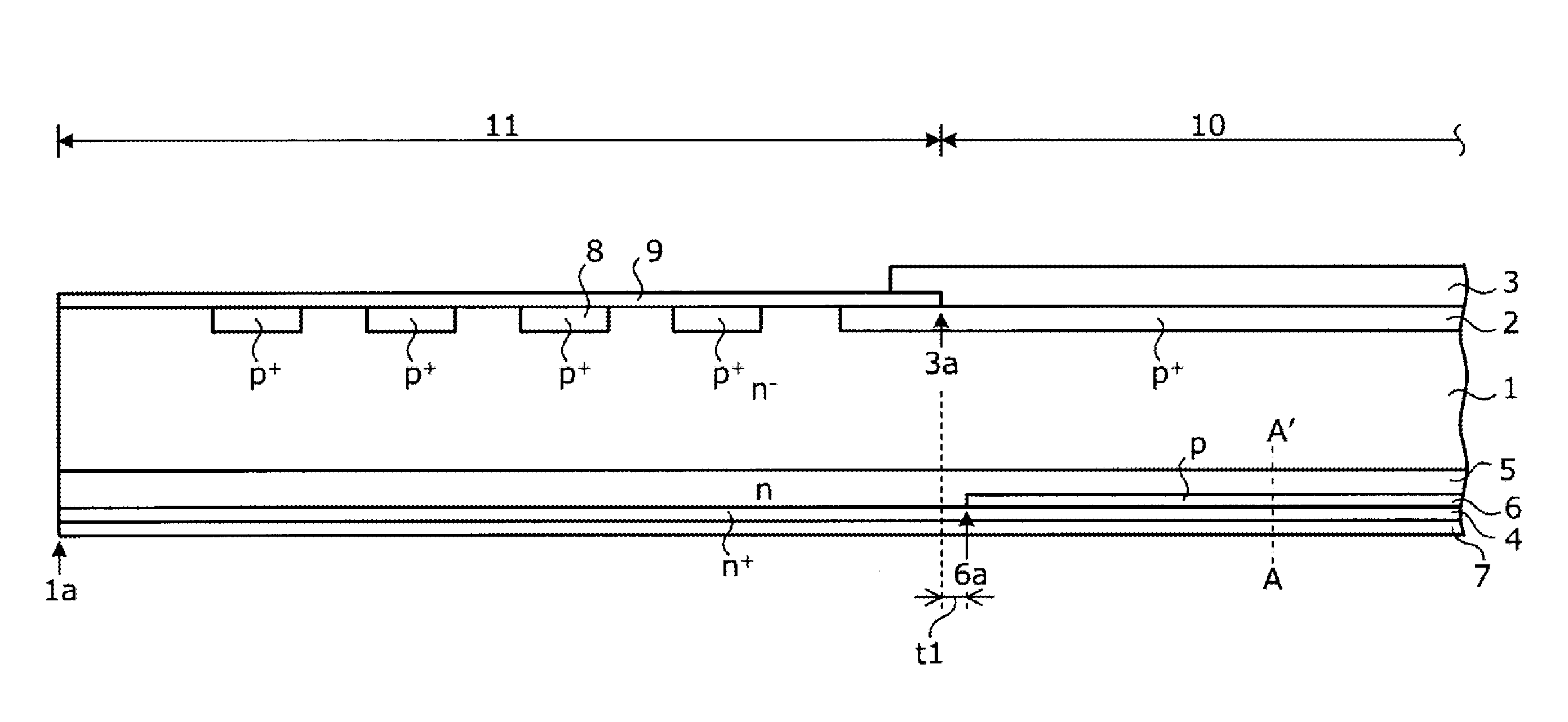
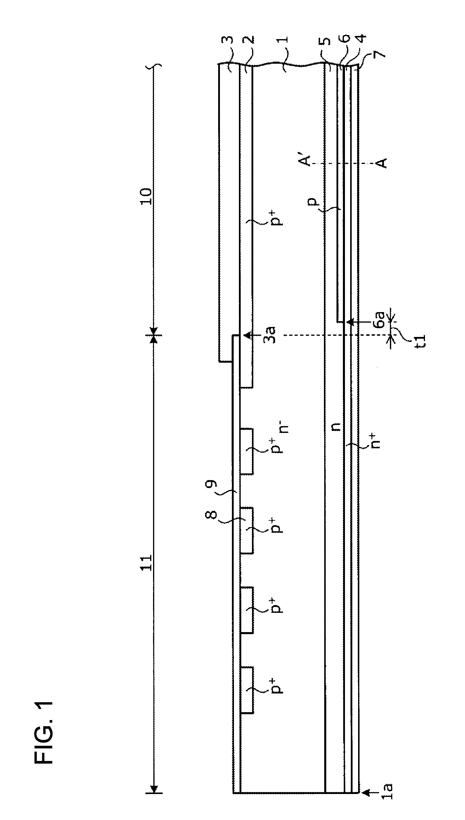
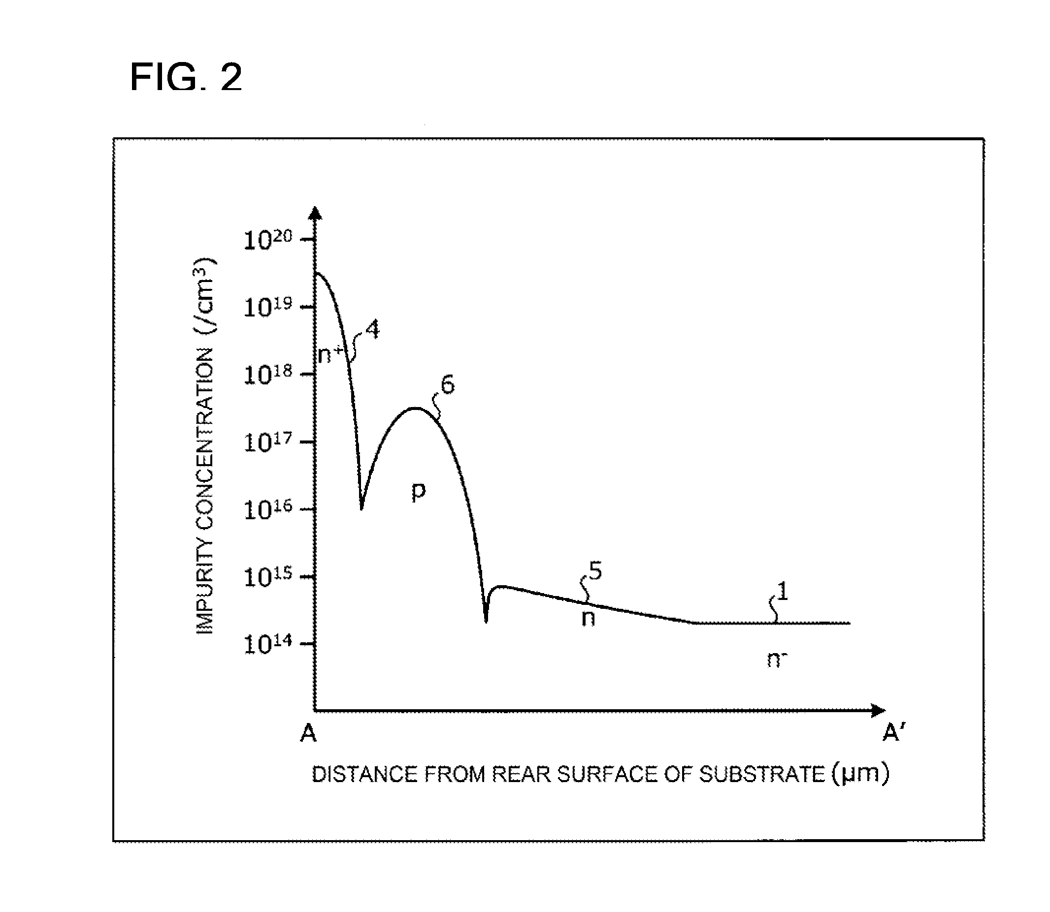
[0063]The structure of a semiconductor device according to Embodiment 1 will be described. FIG. 1 is a cross-sectional view illustrating the structure of the semiconductor device according to Embodiment 1. FIG. 2 is a characteristic diagram illustrating an impurity concentration distribution along the cutting line A-A′ of FIG. 1. In FIG. 2, the horizontal axis indicates the distance from the rear surface of a substrate (an interface between an n+ cathode layer 4 and a cathode electrode 7) in the depth direction of the substrate and the vertical axis indicates impurity concentration along the cutting line A-A′ which traverses a rear-surface-side region of the substrate in the depth direction (which holds for FIGS. 9 and 13. As illustrated in FIG. 1, the semiconductor device according to Embodiment 1 includes an active region 10 and an edge termination structure portion (edge portion) 11 that surrounds the active region 10, which are provided in an n− semiconductor substrate that will...
embodiment 2
[0089]Next, a semiconductor device manufacturing method according to Embodiment 2 will be described. FIG. 6 is a flowchart illustrating the outline of the semiconductor device manufacturing method according to Embodiment 2. The semiconductor device manufacturing method according to Embodiment 2 differs from the semiconductor device manufacturing method according to Embodiment 1 in that, after electron beams are radiated to control the lifetime, an n+ cathode layer 4 is formed and laser annealing is performed to activate the n+ cathode layer 4.
[0090]Specifically, first, similarly to Embodiment 1, a process from the formation of a front surface element structure to the formation of a buried p layer 6 is performed (Steps S11 to S14). Then, after a resist mask used to form the buried p layer 6 is removed, impurities which are implanted by an ion implantation process for forming an n buffer layer 5 and an ion implantation process for forming the buried p layer 6 are thermally diffused by...
embodiment 3
[0092]Next, a semiconductor device manufacturing method according to Embodiment 3 will be described. FIG. 7 is a flowchart illustrating the outline of the semiconductor device manufacturing method according to Embodiment 3. The semiconductor device manufacturing method according to Embodiment 3 differs from the semiconductor device manufacturing method according to Embodiment 2 in that an anode electrode 3 is formed on the front surface of an n− semiconductor substrate before the rear surface of the n− semiconductor substrate is ground to reduce the thickness of the n− semiconductor substrate.
[0093]Specifically, first, a front surface element structure is formed on the front surface of the n− semiconductor substrate which will be an n− drift region 1 (Step S31) and the anode electrode 3 is formed (Step S32). A method for forming the front surface element structure and a method for forming the anode electrode 3 are the same as those in Embodiment 1. Then, similarly to Embodiment 2, a...
PUM
 Abstract
Description
Claims
Application Information
 - Generate Ideas
- Intellectual Property
- Life Sciences
- Materials
- Tech Scout
- Unparalleled Data Quality
- Higher Quality Content
- 60% Fewer Hallucinations
Browse by: Latest US Patents, China's latest patents, Technical Efficacy Thesaurus, Application Domain, Technology Topic, Popular Technical Reports.
© 2025 PatSnap. All rights reserved.Legal|Privacy policy|Modern Slavery Act Transparency Statement|Sitemap|About US| Contact US: help@patsnap.com