Electron emission device and reflex klystron with the same

a technology of electric emission device and reflex klystron, which is applied in the direction of reflex klystron, discharge tube/lamp details, transit-tube cathode, etc., can solve the problems of small current density of electron rejection and large feature siz

Active Publication Date: 2015-12-31
TSINGHUA UNIV +1
View PDF0 Cites 5 Cited by
  • Summary
  • Abstract
  • Description
  • Claims
  • Application Information

AI Technical Summary

Problems solved by technology

However, the traditional reflex klystron adopts silicon tips as the emitter, thus the feature size is large, and the current density of the electron rejection is small.

Method used


Image

  • Electron emission device and reflex klystron with the same
  • Electron emission device and reflex klystron with the same
  • Electron emission device and reflex klystron with the same

Examples


Embodiment Construction

[0019]The disclosure is illustrated by way of example and not by way of limitation in the figures of the accompanying drawings in which like references indicate similar elements. It should be noted that references to “an” or “one” embodiment in this disclosure are not necessarily to the same embodiment, and such references mean at least one.

[0020]References will now be made to the drawings to describe, in detail, various embodiments of the present ionization electron emission device.

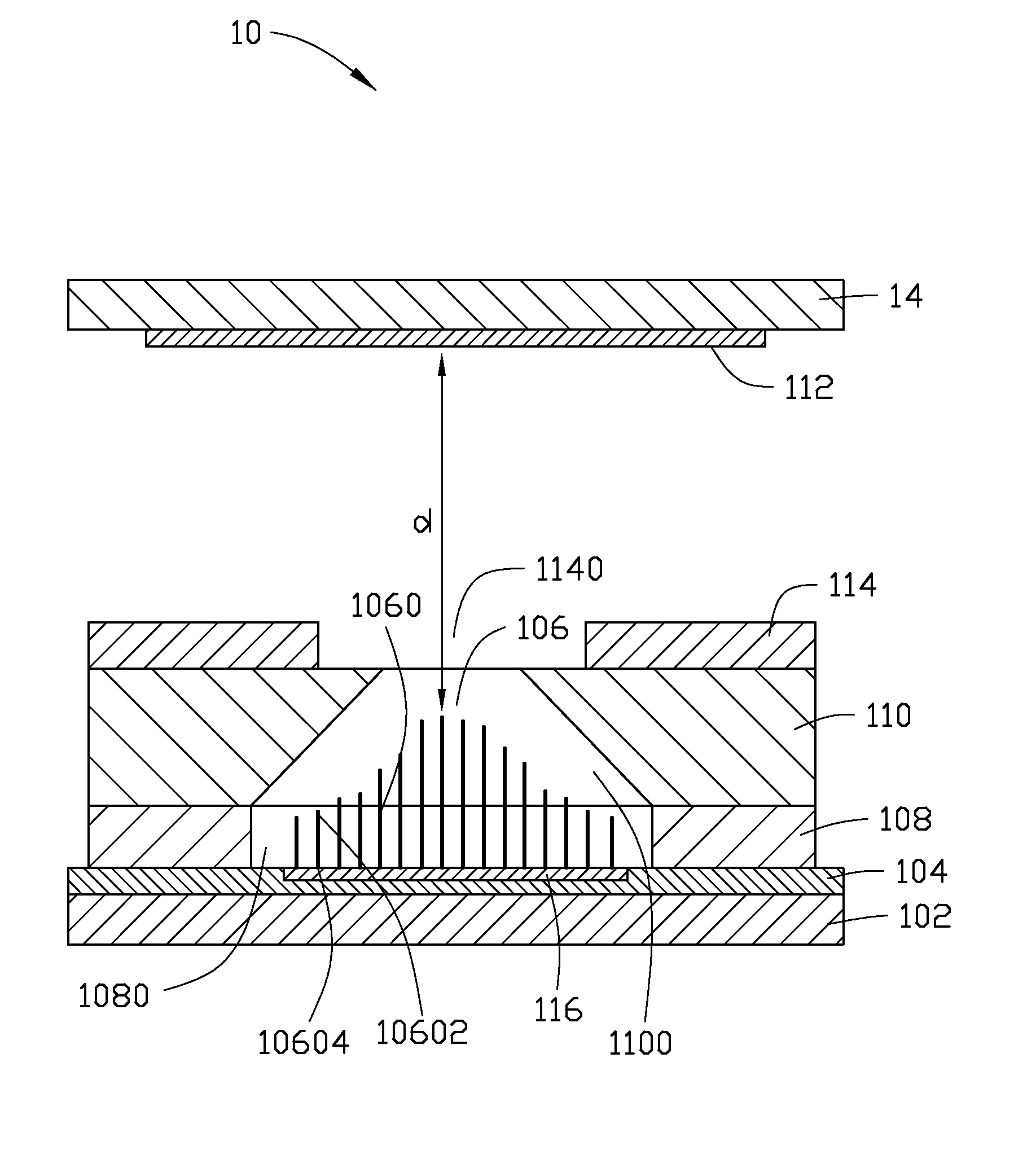
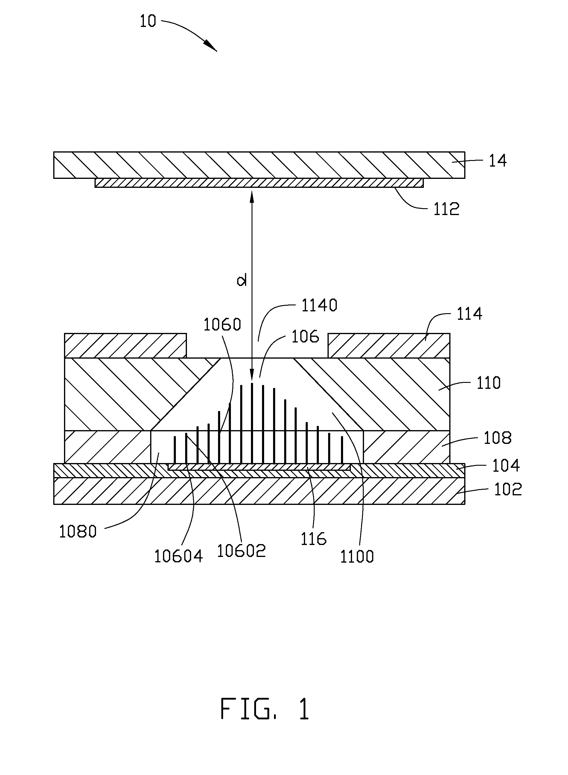
[0021]Referring to FIG. 1, an electron emission device 10 comprises an insulating substrate 102, a cathode 104, an electron emitter structure 106, an insulating layer 108, an electron extraction electrode 110, and an anode 112.

[0022]The cathode 104 is spaced from and opposite to the anode 112. The electrode emitter 106 is electrically connected to the cathode 104. The electron extraction electrode 110 is insulated from the cathode 104 via the insulating layer 108.

[0023]The cathode 104 is located on a sur...


PUM


Abstract

An electron emission device includes an anode, a cathode, an electron emitter structure, and an electron extraction electrode. The cathode is spaced from the anode. The electron emitter structure is electrically connected to the cathode. The electron extraction electrode is insulated from the cathode. The electron extraction electrode defines a through hole surrounded by a sidewall, and the electron emitter structure faces to the sidewall. The electron emitter structure includes a number of electron emitters extending toward the sidewall, each of the number of electron emitters includes an electron emission terminal, a first distance between each electron emission terminal and the sidewall is substantially the same, a second distance between the electron emission terminal and the anode is greater than or equal to 10 micrometers and smaller than or equal to 200 micrometers, and a pressure in the electron emission device is smaller than or equal to 100 Pascal.

Description

CROSS-REFERENCE TO RELATED APPLICATIONS[0001]This application claims all benefits accruing under 35 U.S.C. §119 from China Patent Application No. 201410288346.6, filed on Jun. 25, 2014 in the China Intellectual Property Office, disclosure of which is incorporated herein by reference.BACKGROUND[0002]1. Technical Field[0003]The present disclosure relates to a electron emission device and a reflex klystron with the same.[0004]2. Description of Related Art[0005]In general, the THz wave refers to a electromagnetic wave in which the frequency ranging from 0.3 THz to 3 THz or 0.1 THz to 10 THz. The band of THz wave lies between the infrared wave and the millimeter wave. The THz wave has excellent properties. For example, THz wave has certain ability to penetrate objects, and the photon energy is small, thus the THz will not cause damage to the objects. At the same time, a lot of material can absorb the THz wave.[0006]The reflex klystron is used to emit electromagnetic wave. In order to emi...

Claims


Application Information

Patent Timeline
Patent Type & Authority Applications(United States)
IPC IPC(8): H01J25/22H01J23/08
CPCH01J25/22H01J1/304H01J3/021H01J23/04H01J23/06H01J2201/30469
Inventor LIU, PENGCHEN, PI-JINZHOU, DUAN-LIANGZHANG, CHUN-HAIFAN, SHOU-SHAN
Owner TSINGHUA UNIV
Why Eureka
Try Eureka