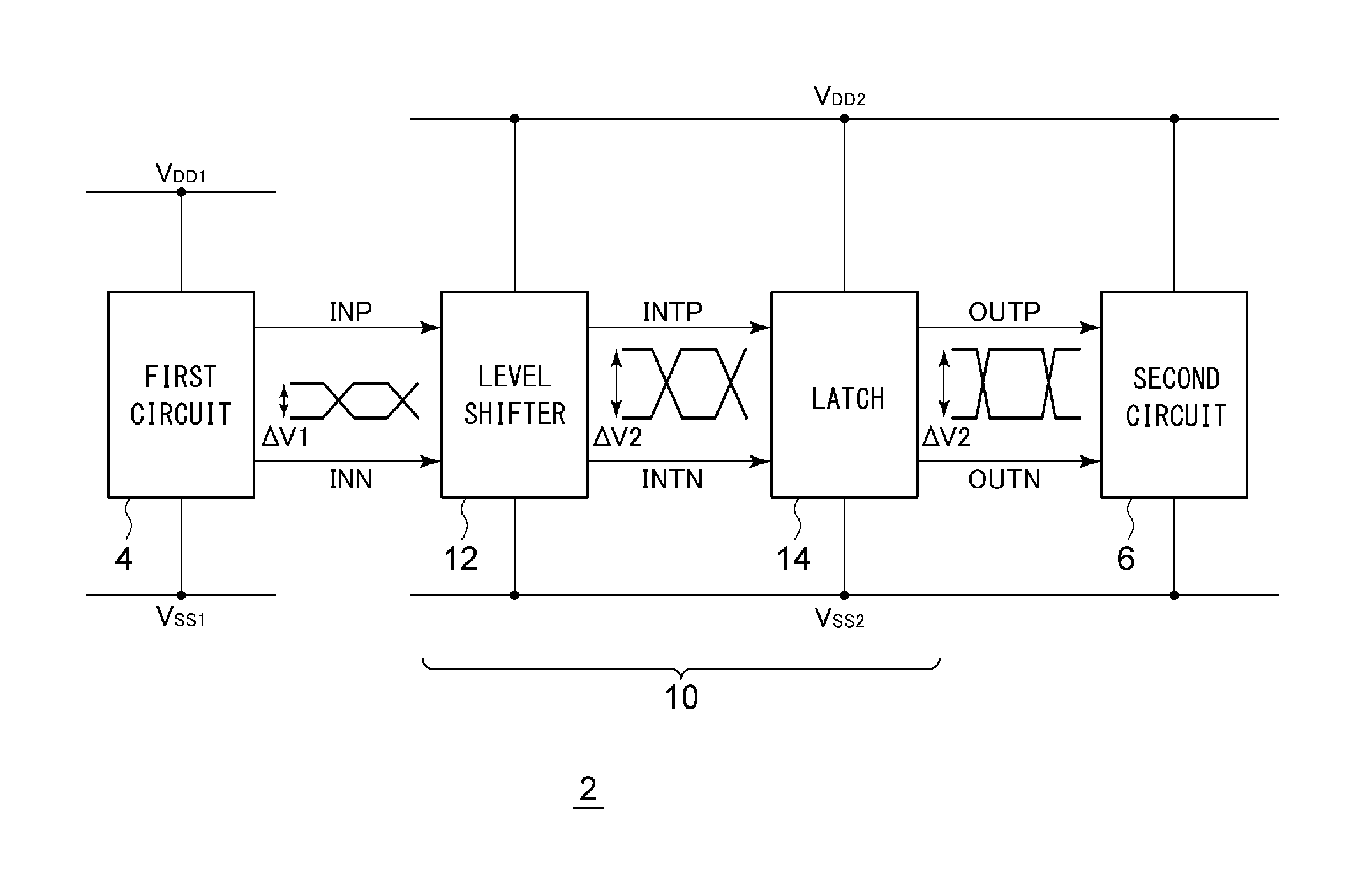
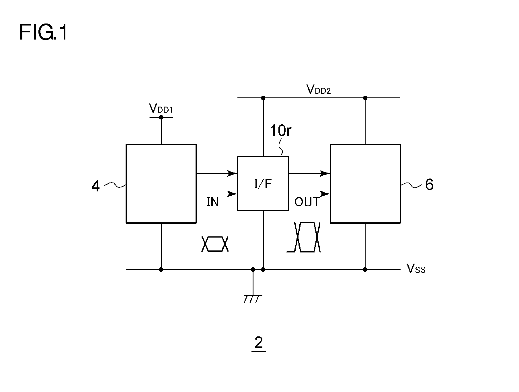
Interface circuit

a technology of interface circuit and interface arrangement, applied in the direction of logic circuit coupling/interface arrangement, pulse manipulation, pulse technique, etc., can solve the problems of large power consumption, unsuitability of arrangement, current loss, etc., and achieve the effect of reducing power consumption and high speed

Active Publication Date: 2015-12-31
ROHM CO LTD
View PDF5 Cites 16 Cited by
  • Summary
  • Abstract
  • Description
  • Claims
  • Application Information

AI Technical Summary

Benefits of technology

[0013]The present invention has been made in order to solve such a problem. Accordingly, it is an exemplary purpose of an embodiment of the present invention to provide an interface circuit which is capable of generating a signal that transits with a high speed, and which is capable of providing reduced power consumption.

Problems solved by technology

Thus, in particular, such an arrangement leads to a problem of current loss due to a through current that occurs when a signal having such a low transition speed propagates through the digital circuit.
The voltage comparator 200 requires the supply of a stationary current Ic regardless of whether or not there is transition of the signal, leading to large power consumption.
Thus, such an arrangement is unsuitable for such a usage having a strong demand for reducing power consumption.
This leads to difficulty in providing reduced power consumption.

Method used


Image

  • Interface circuit
  • Interface circuit
  • Interface circuit

Examples


first modification

[0093]FIG. 8 is a circuit diagram showing the interface circuit 10 according to a first modification. The interface circuit 10 includes the level shifter 12 having a configuration that differs from that shown in FIG. 4.

[0094]The first feature is that the interface circuit 10 further includes a third NMOS transistor MN3 and a fourth NMOS transistor MN4. The third NMOS transistor MN3 is interposed between the first NMOS transistor MN1 and the first PMOS transistor MP1. The positive signal INP of the input signal IN is input to the gate of the third NMOS transistor MN3. The fourth NMOS transistor MN4 is interposed between the second NMOS transistor MN2 and the second PMOS transistor MP2. The negative signal INN of the input signal IN is input to the gate of the fourth NMOS transistor MN4.

[0095]By interposing the NMOS transistors MN3 and MN4 arranged such that the input signal is input to their gates, such an arrangement is capable of reducing the effect on the input signal IN of a para...

second modification

[0099]In FIG. 8, the third NMOS transistor MN3 and the fourth NMOS transistor MN4 may be omitted, and only the fifth PMOS transistor MP5 and the sixth PMOS transistor MP6 may be provided. Conversely, only the third NMOS transistor MN3 and the fourth NMOS transistor MN4 may be provided, and the fifth PMOS transistor MP5 and the sixth PMOS transistor MP6 may be omitted.

third modification

[0100]FIG. 9 is a circuit diagram showing the interface circuit 10 according to a third modification. In this modification, the input signal IN to be received by the level shifter 12 is configured as a binary signal that switches between VDD1 as high level and VSS as low level. The interface circuit 10 has the same basic configuration as that of the interface circuit 10 shown in FIG. 4. That is to say, the interface circuit 10 includes the level shifter 12 configured as an upstream stage and the latch circuit 14 configured as a downstream stage.

[0101]The first CMOS inverter 20 includes the first NMOS transistor MN1 and the first PMOS transistor MP1. The positive signal INP of the input signal IN is input to the gate of the first NMOS transistor MN1. The gate of the first PMOS transistor MP1 is connected to the output of the second CMOS inverter 22.

[0102]Similarly, the second CMOS inverter 22 includes the second NMOS transistor MN2 and the second PMOS transistor MP2. The negative sig...


PUM


Abstract

An interface circuit receives an input signal IN having a first voltage amplitude from a first circuit, and outputs an output signal OUT having a second voltage amplitude to a second circuit. A level shifter comprises a first CMOS inverter and a second CMOS inverter which are cross-coupled, and a current limiting circuit that limits a current that flows through the first CMOS inverter and the second CMOS inverter, and converts the input signal IN into an intermediate signal INT which is a differential signal. A latch circuit receives the intermediate signal INT from the level shifter, and switches its state according to the positive signal and the negative signal of the intermediate signal INT.

Description

CROSS-REFERENCE TO RELATED APPLICATIONS[0001]This application is based upon and claims the benefit of priority from the prior Japanese Patent Application No. 2014-130714, filed on Jun. 25, 2014, the entire contents of which are incorporated herein by reference.BACKGROUND OF THE INVENTION[0002]1. Field of the Invention[0003]The present invention relates to an interface circuit that allows a digital signal to be supplied or received between two circuit blocks.[0004]2. Description of the Related Art[0005]In recent years, there has been an increased demand for a technique for providing a semiconductor integrated circuit or a circuit system (which will collectively be referred to as a “semiconductor integrated circuit” hereafter) with reduced power consumption. In order to meet such a demand, the semiconductor integrated circuit is configured as multiple circuit blocks, and is configured such that each circuit block operates with a different optimum voltage amplitude or otherwise with a ...

Claims


Application Information

Patent Timeline
Patent Type & Authority Applications(United States)
IPC IPC(8): H03K19/0185H03K19/0175H03K19/00
CPCH03K19/018521H03K3/35613H03K19/017509H03K19/0005
Inventor TSUJI, MASANOBU
Owner ROHM CO LTD
Why Eureka
Try Eureka