

Ultra-conformal carbon film deposition layer-by-layer deposition of carbon-doped oxide films
a carbon film, ultra-conform technology, applied in the direction of coatings, chemical vapor deposition coatings, metallic material coating processes, etc., can solve the problems of poor deposited material quality, incompatibility of hard mask spacers with high temperature applications, and inability to reliably form photolithographic techniques
- Summary
- Abstract
- Description
- Claims
- Application Information
AI Technical Summary
Benefits of technology
Problems solved by technology
Method used
Image

Examples
Embodiment Construction
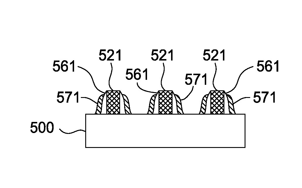
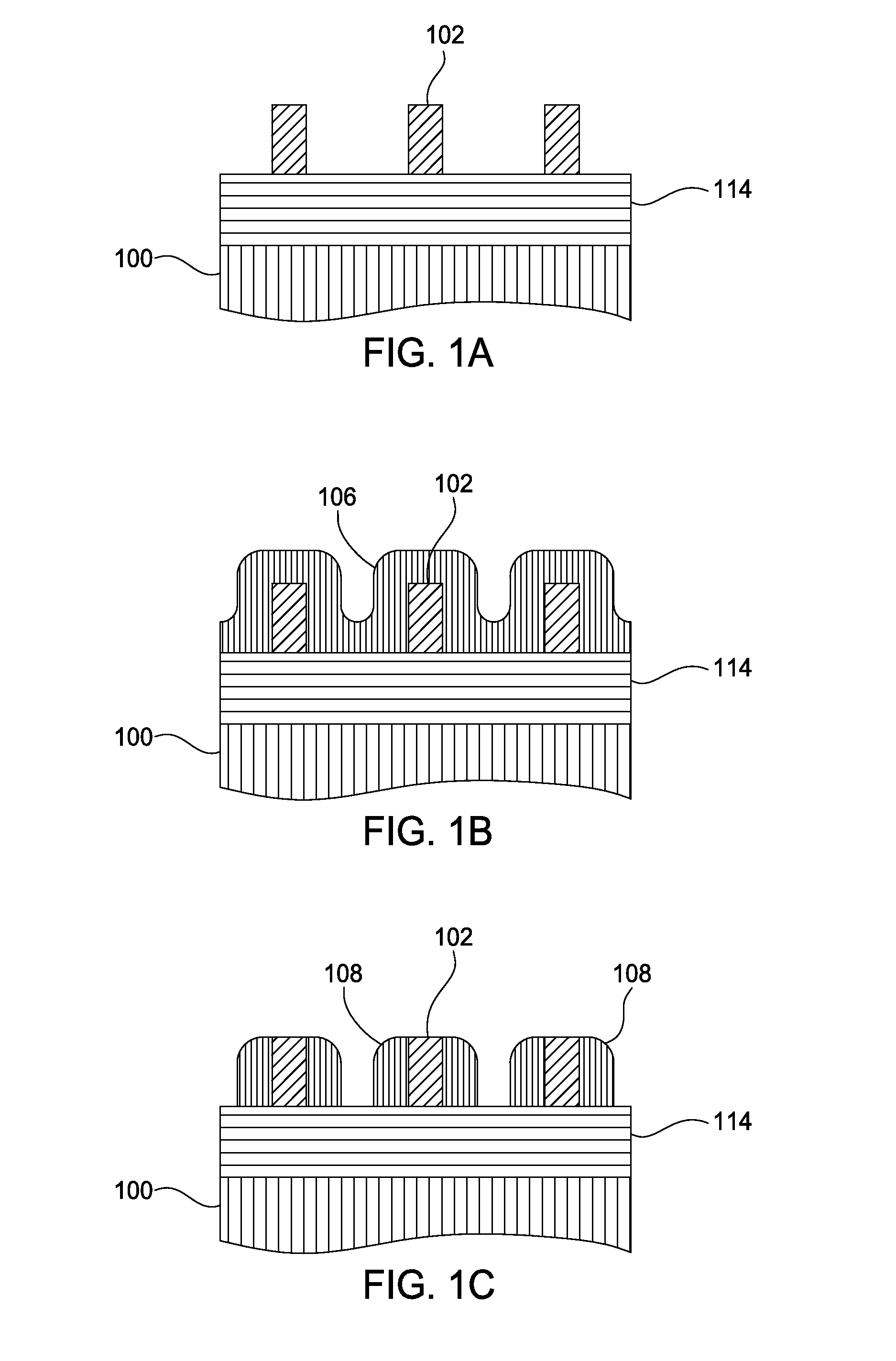
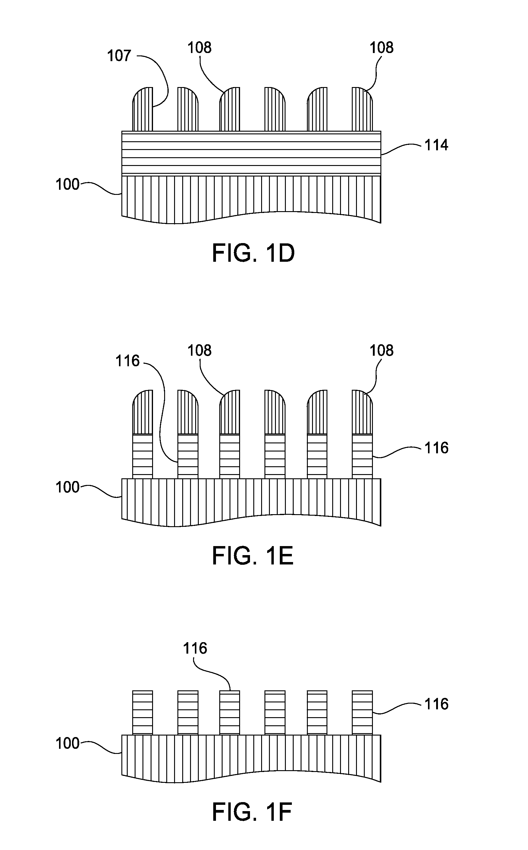
[0017]Embodiments of the present invention relate to deposition of an ultra-conformal carbon-based material. In various embodiments, an ultra-conformal carbon-based material, such as amorphous carbon, is deposited over features of sacrificial structure material patterned using a high-resolution photomask. In one example, the ultra-conformal carbon-based material serves as a protective layer during an ashing or etching process, leaving the sacrificial structure material with an upper surface exposed and sidewalls protected by the carbon-based spacers. Upon removal of the sacrificial structure material, the remaining carbon-based spacers may perform as a hardmask layer for etching the underlying layer or structure. While the process described herein is mainly related to a spacer application using carbon-based material, the improved process of the invention is also applicable to other applications which may require a conformal amorphous carbon film such as gap fill, hard mask for hot i...
PUM
| Property | Measurement | Unit |
|---|---|---|
| temperature | aaaaa | aaaaa |
| temperature | aaaaa | aaaaa |
| pressure | aaaaa | aaaaa |
Abstract
Description
Claims
Application Information