Organic electroluminescence display panel

Active Publication Date: 2016-01-07
AU OPTRONICS CORP
View PDF0 Cites 13 Cited by
  • Summary
  • Abstract
  • Description
  • Claims
  • Application Information

AI Technical Summary

Benefits of technology

[0007]The invention is directed to an organic electroluminescence display panel that allows the number of times of using the

Problems solved by technology

Nevertheless, the FMM technique is not cost effective, and

Method used


Image

  • Organic electroluminescence display panel
  • Organic electroluminescence display panel
  • Organic electroluminescence display panel

Examples


first embodiment

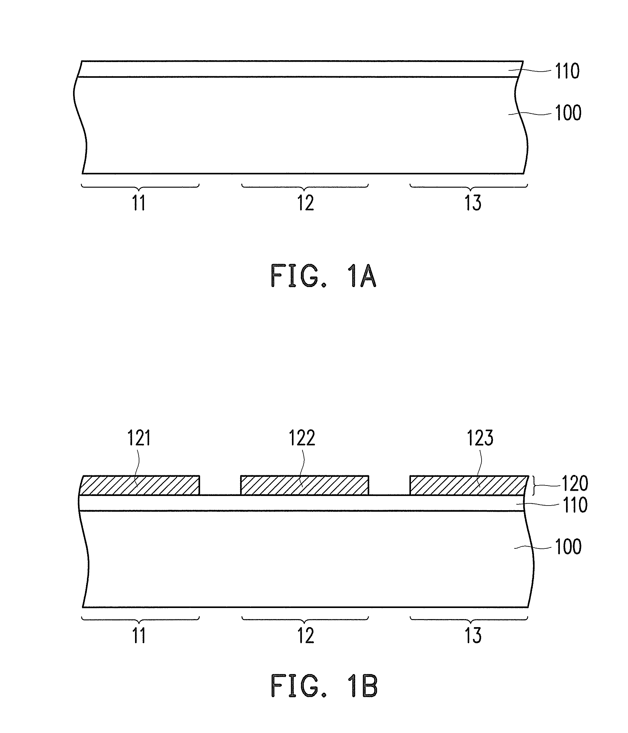
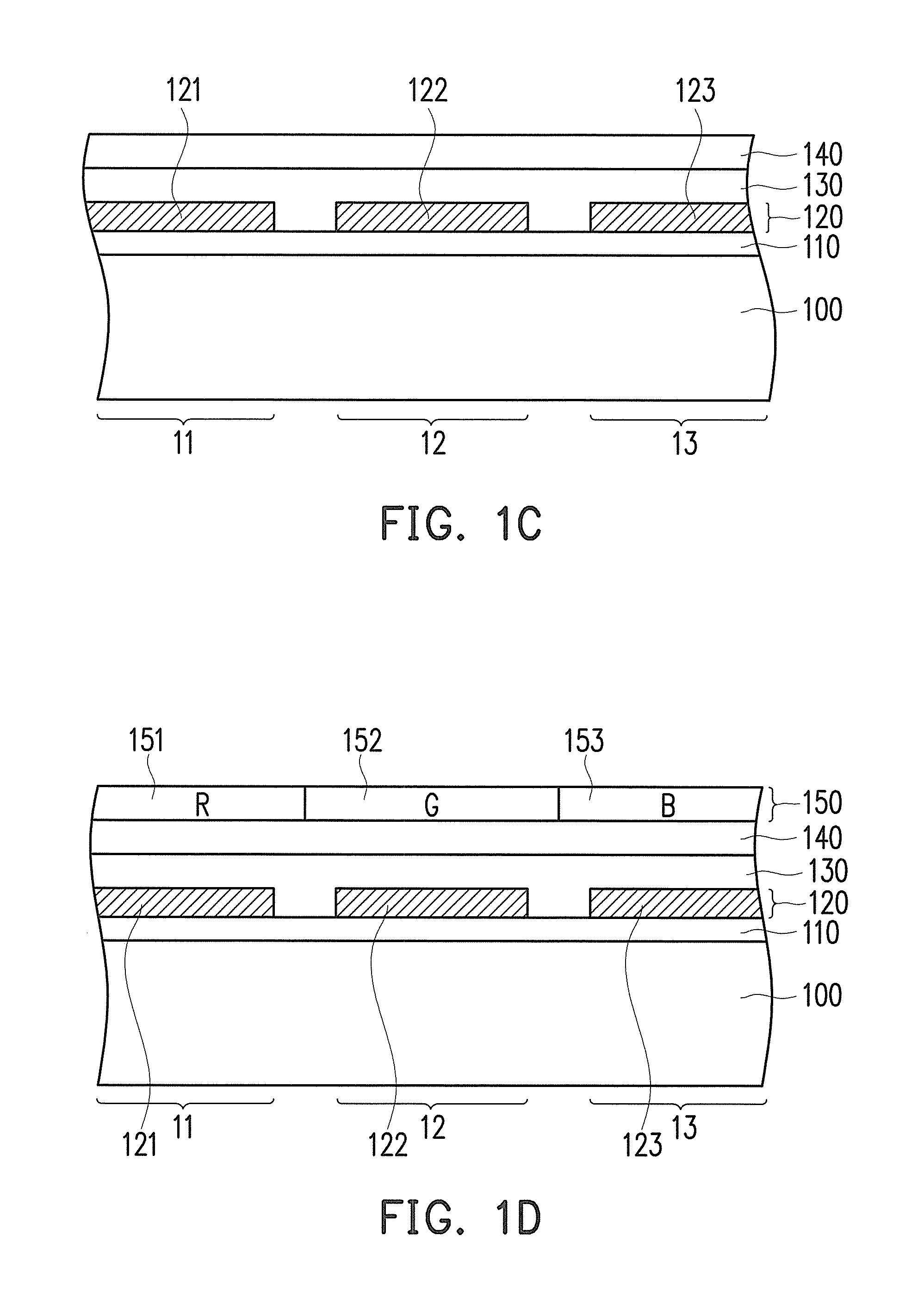
[0017]FIG. 1A to FIG. 1F are schematic cross-sectional flow charts illustrating a manufacturing process of an organic electroluminescence display panel according to the invention. FIG. 2 is a schematic top view illustrating the device layer depicted in FIG. 1A. With reference to FIG. 1A, a device layer 110 is formed on a substrate 100. Here, the substrate 100 is a rigid substrate (e.g., a glass substrate) or a flexible substrate (e.g., a plastic substrate). The substrate 100 may be made of a transparent material or a non-transparent material. Besides, the substrate 100 mainly serves to carry light emitting devices of the organic electroluminescence display panel. Note that the substrate 100 includes a plurality of first pixel areas 11, a plurality of second pixel areas 12, and a plurality of third pixel areas 13, and these pixel areas 11, 12, and 13 respectively display different primary colors of light. To clearly illustrate the invention, FIG. 1A shows one first pixel area 11, one...

second embodiment

[0033]FIG. 3 is a schematic cross-sectional view illustrating an organic electroluminescence display panel according to the invention. The organic electroluminescence display panel 20 depicted in FIG. 3 is similar to the organic electroluminescence display panel 10 depicted in FIG. 1F, while the difference therebetween lies in that the light emitting layer 250 is directly formed on the first electrode layer 120, and the second electrode layer 170 is directly formed on the light emitting layer 250 according to the present embodiment. The organic layer 101 is formed of the light emitting layer 250. Similarly, the light emitting layers 251, 252, and 253 are respectively located in the first, second, and third pixel areas 21, 22, and 23. For instance, the light emitting layers 251, 252, and 253 may be respectively formed by performing an evaporation process with use of first, second, and third FMMs, which should however not be construed as a limitation to the invention. The light emitti...

third embodiment

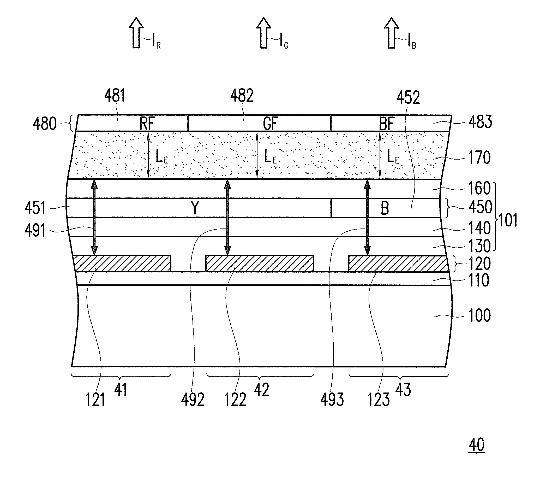
[0038]FIG. 4 is a schematic cross-sectional view illustrating an organic electroluminescence display panel according to the invention. The organic electroluminescence display panel 30 depicted in FIG. 4 is similar to the organic electroluminescence display panel 10 depicted in FIG. 1F, while the difference therebetween lies in that the organic layer 101 includes the light emitting layer 350, and the distribution of the color light emitting materials in the light emitting layer 350 is different. With reference to FIG. 4, the light emitting layer 350 includes light emitting layers 351, 352, and 353 respectively located in the first, second, and third pixel areas 31, 32, and 33, and the light emitting layer 353 covers the light emitting layers 351 and 352. According to the present embodiment, the first color light emitting material is a red light emitting material R, the second color light emitting material is a green light emitting material G, and the third color light emitting materi...


PUM


Abstract

An organic electroluminescence display panel that includes a plurality of first pixel areas, a plurality of second pixel areas, and a plurality of third pixel areas is provided. The organic electroluminescence display panel includes a first electrode layer, an organic layer including a light-emitting layer made of organic light-emitting material and a second electrode layer. The first electrode layer includes a reflective material. The organic layer is located on the first electrode layer. The second electrode layer is located on the organic layer. The material of the second electrode layer includes a transparent metal oxide conductive material. The thickness of the second electrode layer is a single thickness and is greater than 300 nm.

Description

BACKGROUND[0001]1. Field[0002]The invention relates to a display panel. More particularly, the invention relates to an organic electroluminescence display panel.[0003]2. Description of Related Art[0004]An organic electroluminescence display panel (e.g., an organic light emitting diode (OLED) display panel) characterized by active light emission, high contrast ratio, small thickness, and wide view angle is likely to become one of the mainstream new-generation flat panel displays.[0005]In the organic electroluminescence display panel, a top emissive OLED can have high efficiency and high color saturation because the top emissive OLED achieves significant resonant cavity effects. For the purpose of accomplishing the resonant cavity effects, an organic layer including a light-emitting layer made of organic light-emitting material in the conventional organic electroluminescence display panel often requires the use of a fine metal mask (FMM) to adjust the light color and the light intensi...

Claims


Application Information

Patent Timeline
IPC IPC(8): H01L27/32H01L51/50H01L51/52
CPCH01L27/3209H01L51/504H01L51/5218H01L2251/558H01L51/5206H01L51/5221H01L27/322H01L51/5234H10K59/35H10K59/38H10K50/818H10K50/828H10K50/852H10K2102/3026H10K2102/351H10K71/00H10K59/32H10K50/13H10K50/81H10K50/82
Inventor HUANG, CHIH-ANCHANG, HUNG-YILIN, PEI-LINGTSAI, LUN
Owner AU OPTRONICS CORP
Why Eureka
Try Eureka