Buffer amplifier and trans-impedance amplifier including the same

a buffer amplifier and amplifier technology, applied in the field of transimpedance amplifiers, can solve the problems of inability to perform normal signal processing on another ic chip, inability to achieve high-speed operation of inverter-type buffer amplifiers, and loss of voltage in the ic chip, so as to improve signal delivery performance, reduce input capacitance, and low distortion characteristics

Active Publication Date: 2016-01-07
ELECTRONICS & TELECOMM RES INST
View PDF4 Cites 12 Cited by
  • Summary
  • Abstract
  • Description
  • Claims
  • Application Information

AI Technical Summary

Benefits of technology

[0011]The present invention provides a buffer amplifier having improved signal delivery performance and reduced input capacitance, providing linearity, and having low distortion characteristics and a trans-impedance amplifier including the buffer amplifier.

Problems solved by technology

When a buffer amplifier is not provided to the IC chip, voltage drop may occur in the IC chip due to the influence of the another IC chip connected to the final terminal.
Accordingly, a signal is not normally delivered to the another IC chip connected to the final terminal and the another IC chip may not perform normal signal processing.
However, since an input impedance and an output impedance of the inverter-type buffer amplifier have high values, the inverter-type buffer amplifier is not suitable for a high-speed operation.
Moreover, the inverter-type buffer amplifier consumes a lot of current and it is difficult to apply the inverter-type buffer amplifier to a differential structure.
However, the ECL-type buffer amplifier has a low voltage gain.
Additionally, the CML-type buffer amplifier has poor gain flatness and large voltage drop, so that it cannot raise output voltage.
However, in order to improve current driving characteristics, if the areas of input transistors in a buffer amplifier of a TIA are designed larger, the bandwidth of the TIA is limited.
That is, the distortion of the chip power of the TIA may be fed back to the other components of the TIA and due to this, a signal processed by the components of the TIA may be distorted.

Method used


Image

  • Buffer amplifier and trans-impedance amplifier including the same
  • Buffer amplifier and trans-impedance amplifier including the same
  • Buffer amplifier and trans-impedance amplifier including the same

Examples


Embodiment Construction

[0035]Hereinafter, embodiments of the present invention will be described with reference to the accompanying drawings. Rather, these embodiments are provided so that this disclosure will be thorough and complete, and will fully convey the scope of the inventive concept to those skilled in the art.

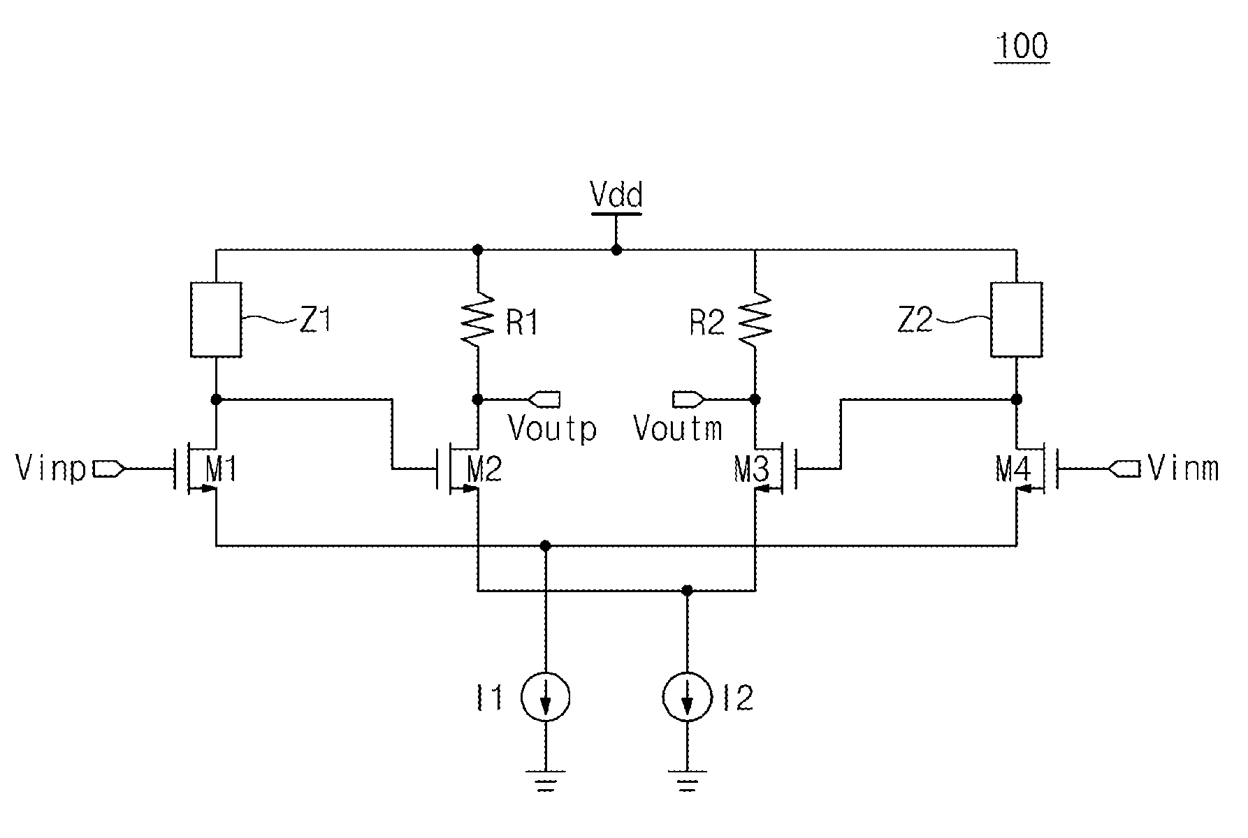
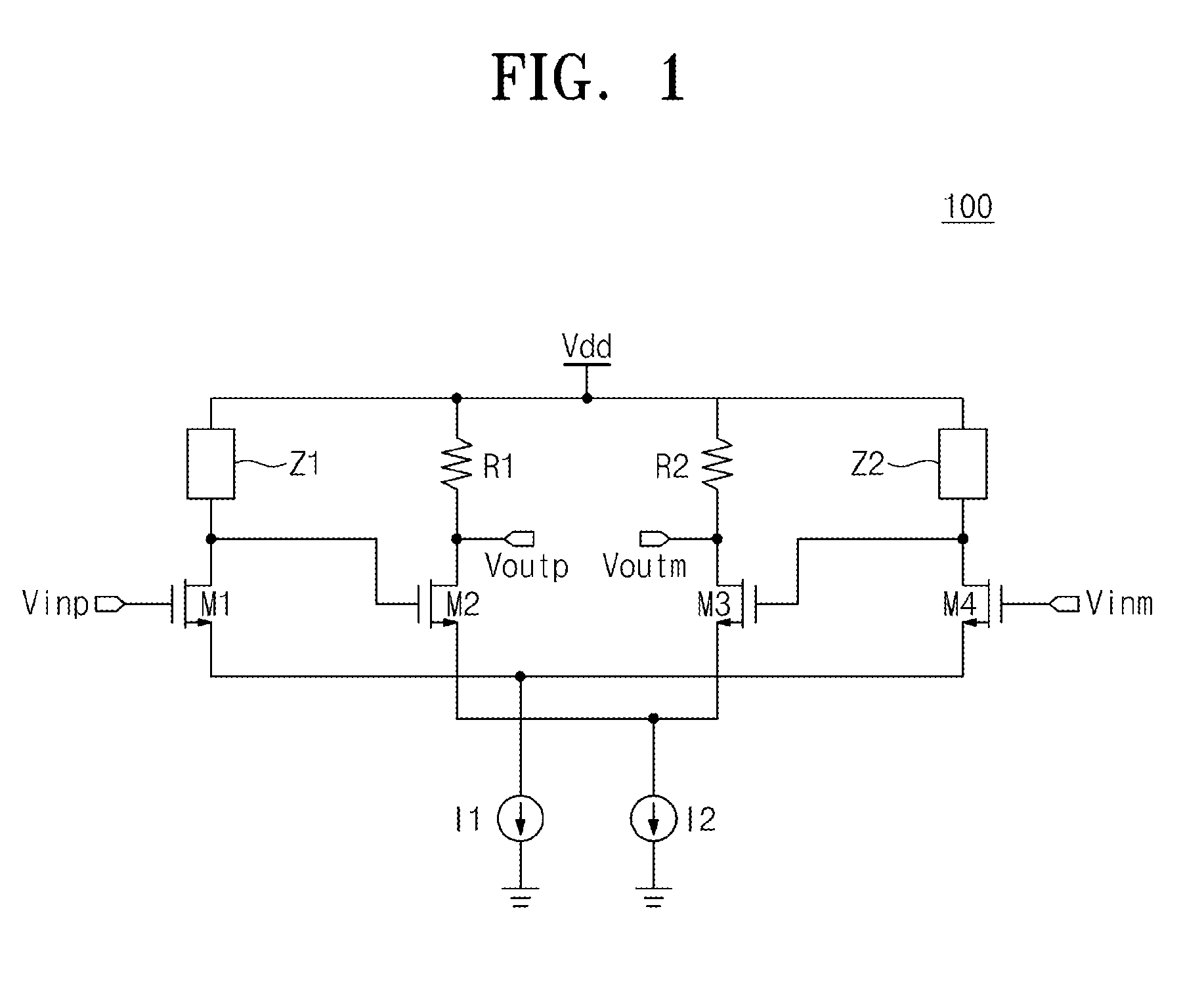
[0036]FIG. 1 is circuit diagram illustrating an exemplary buffer amplifier 100. Referring to FIG. 1, the buffer amplifier 100 includes first to fourth transistors M1 to M4, first and second current sources I1 and I2, first and second impedance elements Z1 and Z2, and first and second resistance elements R1 and R2.

[0037]The first current source I1 is connected between sources of the first and fourth transistors M1 and M4 and a ground node. The second current source I2 is connected between sources of the second and third transistors M2 and M3 and the ground node. The ground node is a node where ground voltage Vss is supplied.

[0038]Gates of the first and fourth transistors M1 and M4 are connec...


PUM


Abstract

Provided is a buffer amplifier. The buffer amplifier includes: a replica bias unit dividing an internal power voltage received from an internal power node to generate a bias voltage; an input unit including a first differential amplifier comparing a first differential input signal with the bias voltage to output a first internal signal and a second differential amplifier comparing a second differential input signal with the bias voltage to output a second internal signal; and an output unit including a third differential amplifier comparing the first internal signal with the second internal signal to output a first differential output signal and a second differential output signal.

Description

CROSS-REFERENCE TO RELATED APPLICATIONS[0001]This U.S. non-provisional patent application claims priority under 35 U.S.C. §119 of Korean Patent Application No. 10-2014-0084322, filed on Jul. 7, 2014, the entire contents of which are hereby incorporated by reference.BACKGROUND OF THE INVENTION[0002]The present invention disclosed herein relates to an electronic device, and more particularly, to a trans-impedance amplifier including the same.[0003]Typically, an integrated circuit (IC) chip includes a buffer amplifier. The buffer amplifier is provided at the final terminal of the IC, for example, an output terminal. The buffer amplifier is configured to prevent an input impedance of another IC chip from affecting the IC chip, for example, a circuit connected to the final terminal of the IC chip. For example, the buffer amplifier is configured to have low output impedance and high current driving characteristics.[0004]When a buffer amplifier is not provided to the IC chip, voltage drop ...

Claims


Application Information

Patent Timeline
Patent Type & Authority Applications(United States)
IPC IPC(8): H03F1/02H03F1/32H03F1/56H03F3/45
CPCH03F1/0205H03F3/45179H03F2203/45112H03F1/3205H03F1/56H03F1/086H03F1/3211H03F3/45183H03F3/45197H03F3/45748H03F2200/387H03F2200/405H03F2200/453H03F2203/45296H03F2203/45301H03F2203/45374H03F2203/45644H03F2203/45652H03F2203/45702
Inventor KIM, YOUNG HOLEE, SANG SOO
Owner ELECTRONICS & TELECOMM RES INST
Why Eureka
Try Eureka