Non-volatile boolean logic operation circuit and operation method thereof

Active Publication Date: 2016-01-21
HUAZHONG UNIV OF SCI & TECH
View PDF7 Cites 22 Cited by
  • Summary
  • Abstract
  • Description
  • Claims
  • Application Information

AI Technical Summary

Benefits of technology

[0119]The logic circuit with two resistive switching elements of the invention is capable of facilitating at least sixteen types of fundamental Boolean logic operation, and results of the logic operation are directly stored in impedance states of the resistive switc

Problems solved by technology

However, the circuit cannot completely realize all sixteen types of Boolean logics, and storage states of

Method used


Image

  • Non-volatile boolean logic operation circuit and operation method thereof
  • Non-volatile boolean logic operation circuit and operation method thereof
  • Non-volatile boolean logic operation circuit and operation method thereof

Examples


first embodiment

[0139]FIG. 5 is a schematic diagram of a non-volatile Boolean logic operation circuit of a first exemplary embodiment of the invention. For the purpose of clear illustration and as an example, a resistive switching element is labeled as a memristor. It can be understood by those skilled in the art that the resistive switching element can be a magnetic random access memory (comprising a spin transfer torque magnetic random access memory (STT-MRAM), a magnetic tunnel junction element (MTJ), a spin valve and so on), a resistive memory, a phase change memory, or other types of resistive switching elements that are capable of reversely changing states in the high resistance state or the low resistance state. As shown in FIG. 5, the logic operation circuit of the first embodiment comprises a first resistive switching element M1, and a second resistive switching element M2.

[0140]A first end 511 of the first resistive switching element M1 operates as a first input end of the logic operation...

second embodiment

[0199]FIG. 7 is a schematic diagram of a non-volatile Boolean logic operation circuit of a second exemplary embodiment of the invention. For the purpose of clear illustration and as an example, a resistive switching element is labeled as a memristor in FIG. 7. It can be understood by those skilled in the art that the resistive switching element can be a magnetic random access memory (comprising a spin transfer torque magnetic random access memory (STT-MRAM), a magnetic tunnel junction element (MTJ), a spin valve an so on), a resistive memory, a phase change memory, or other types of resistive switching elements that are capable of reversely changing states in the high resistance state or the low resistance state. As shown in FIG. 7, the logic operation circuit of the second embodiment comprises a third resistive switching element M3, and a fourth resistive switching element M4.

[0200]A first end 712 of the third resistive switching element M3 operates as a first input end of the logi...

third embodiment

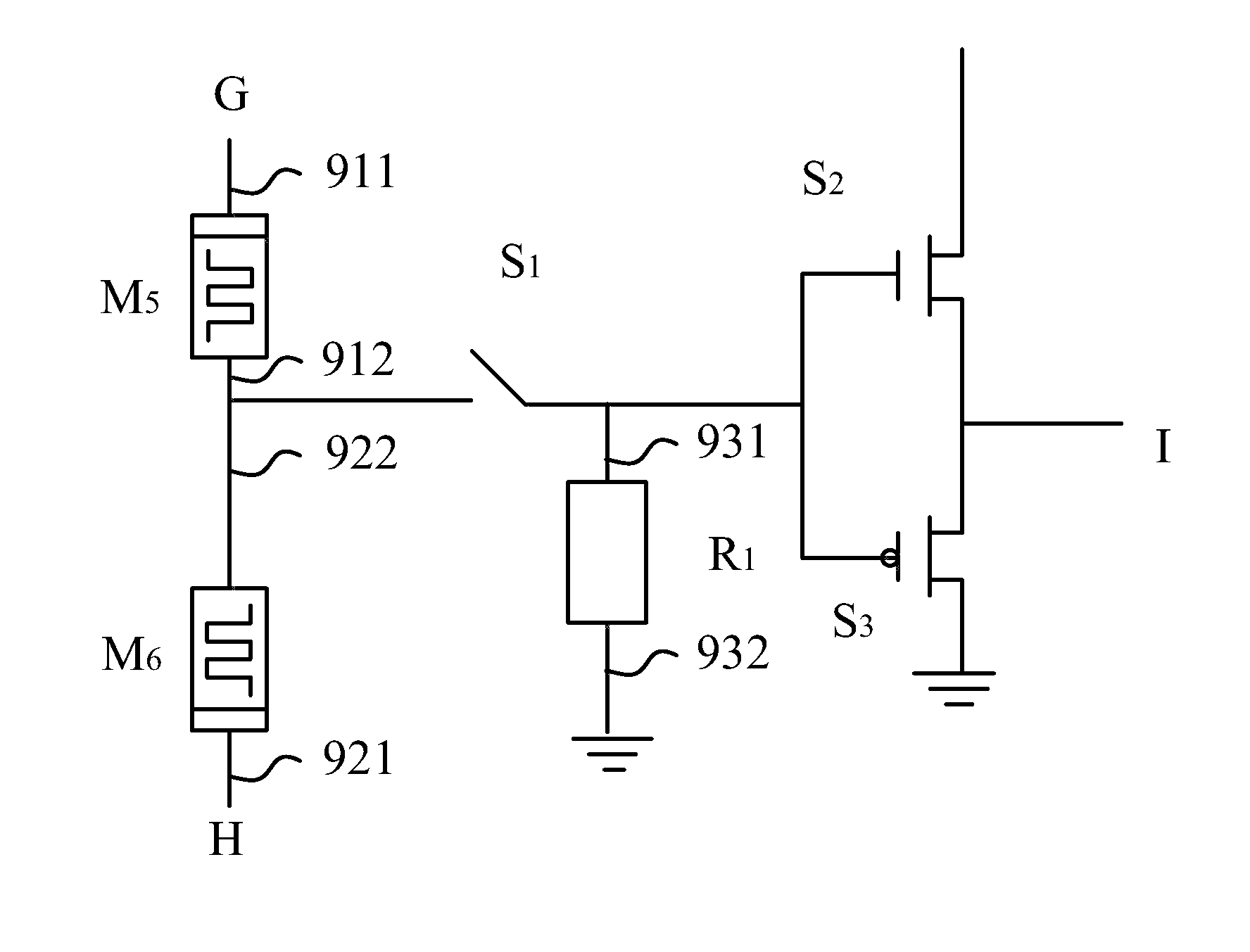
[0276]FIG. 10 illustrates a schematic diagram of a non-volatile Boolean logic operation circuit of a fourth exemplary embodiment of the invention. Difference between this embodiment and the third embodiment in FIG. 9 is that, in this embodiment, the voltage converter is formed by a pair of voltage control switches. In this embodiment, the voltage control switch is a field effect transistor. Referring to FIG. 10, the non-volatile Boolean logic operation circuit of this embodiment comprises: a fifth resistive switching element M5, an sixth resistive switching element M6, a first resistor R1 (voltage dividing resistor), a field effect transistor S1, a field effect transistor S2, and a field effect transistor S3. The field effect transistor S2 and the field effect transistor S3 form a voltage converter, and a polarity of the field effect transistor S2 is opposite to that of the field effect transistor S3, namely, if the field effect transistor S2 employs a N-type field effect transistor...


PUM


Abstract

A non-volatile Boolean logic operation circuit, including: two input ends; an output end; a first resistive switching element M1, the first resistive switching element M including a positive electrode and a negative electrode; and a second resistive switching element M2, the second resistive switching element M2 including a positive electrode and a negative electrode. The negative electrode of the first resistive switching element M1 operates as a first input end of the logic operation circuit. The negative electrode of the second resistive switching element M2 operates as a second input end of the logic operation circuit. The positive electrode of the second resistive switching element M2 is connected to the positive electrode of the first resistive switching element M1, and a connected end thereof operates as the output end of the logic operation circuit.

Description

CROSS-REFERENCE TO RELATED APPLICATIONS[0001]This application is a continuation-in-part of International Patent Application No. PCT / CN2014 / 081870 with an international filing date of Jul. 9, 2014, designating the United States, now pending, and further claims priority benefits to Chinese Patent Application No. 201410279445.8 filed Jun. 20, 2014. The contents of all of the aforementioned applications, including any intervening amendments thereto, are incorporated herein by reference. Inquiries from the public to applicants or assignees concerning this document or the related applications should be directed to: Matthias Scholl P. C., Attn.: Dr. Matthias Scholl Esq., 245 First Street, 18th Floor, Cambridge, Mass. 02142.BACKGROUND OF THE INVENTION[0002]1. Field of the Invention[0003]The invention relates to a non-volatile Boolean logic operation circuit and an operation method thereof.[0004]2. Description of the Related Art[0005]Typically, a logic gate circuit adopts a memristor, a unid...

Claims


Application Information

Patent Timeline
IPC IPC(8): H03K19/00H03K19/20
CPCH03K19/20H03K19/0002H03K19/0021H03K19/0813
Inventor MIAO, XIANGSHUIZHOU, YAXIONGLI, YISUN, HUAJUN
Owner HUAZHONG UNIV OF SCI & TECH
Why Eureka
Try Eureka