Semiconductor memory devices and memory systems including the same

a memory device and semiconductor technology, applied in the field of memory devices, can solve the problem that the ber of memory cells in the drams may rapidly increase, and achieve the effect of enhancing performan

Active Publication Date: 2016-02-11
SAMSUNG ELECTRONICS CO LTD
View PDF10 Cites 40 Cited by
  • Summary
  • Abstract
  • Description
  • Claims
  • Application Information

AI Technical Summary

Benefits of technology

[0006]Some example embodiments may provide a semicond

Problems solved by technology

As the semiconductor fabrication process for volatile memory devices, such as DRAMs, continues to improve, thereb

Method used


Image

  • Semiconductor memory devices and memory systems including the same
  • Semiconductor memory devices and memory systems including the same
  • Semiconductor memory devices and memory systems including the same

Examples


Embodiment Construction

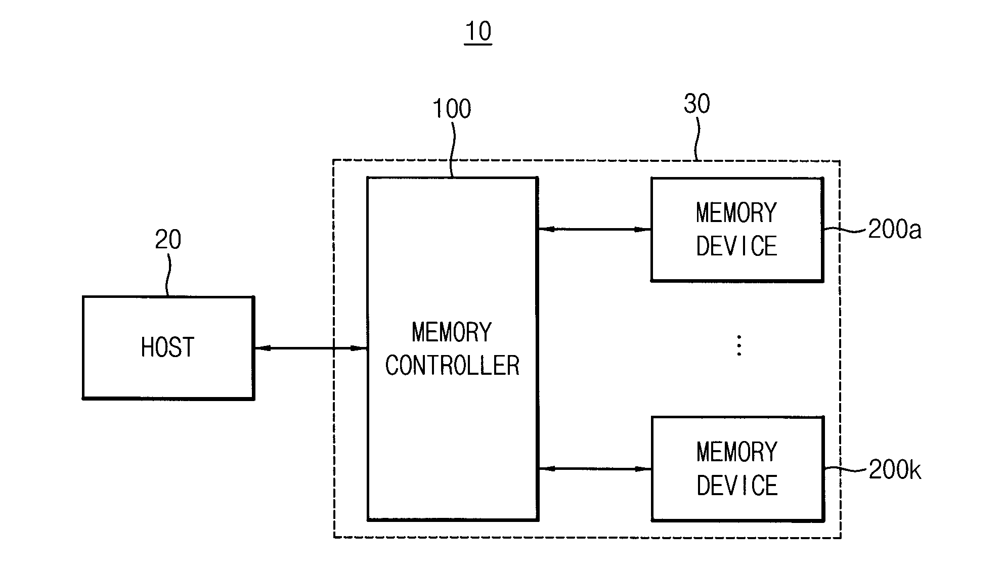
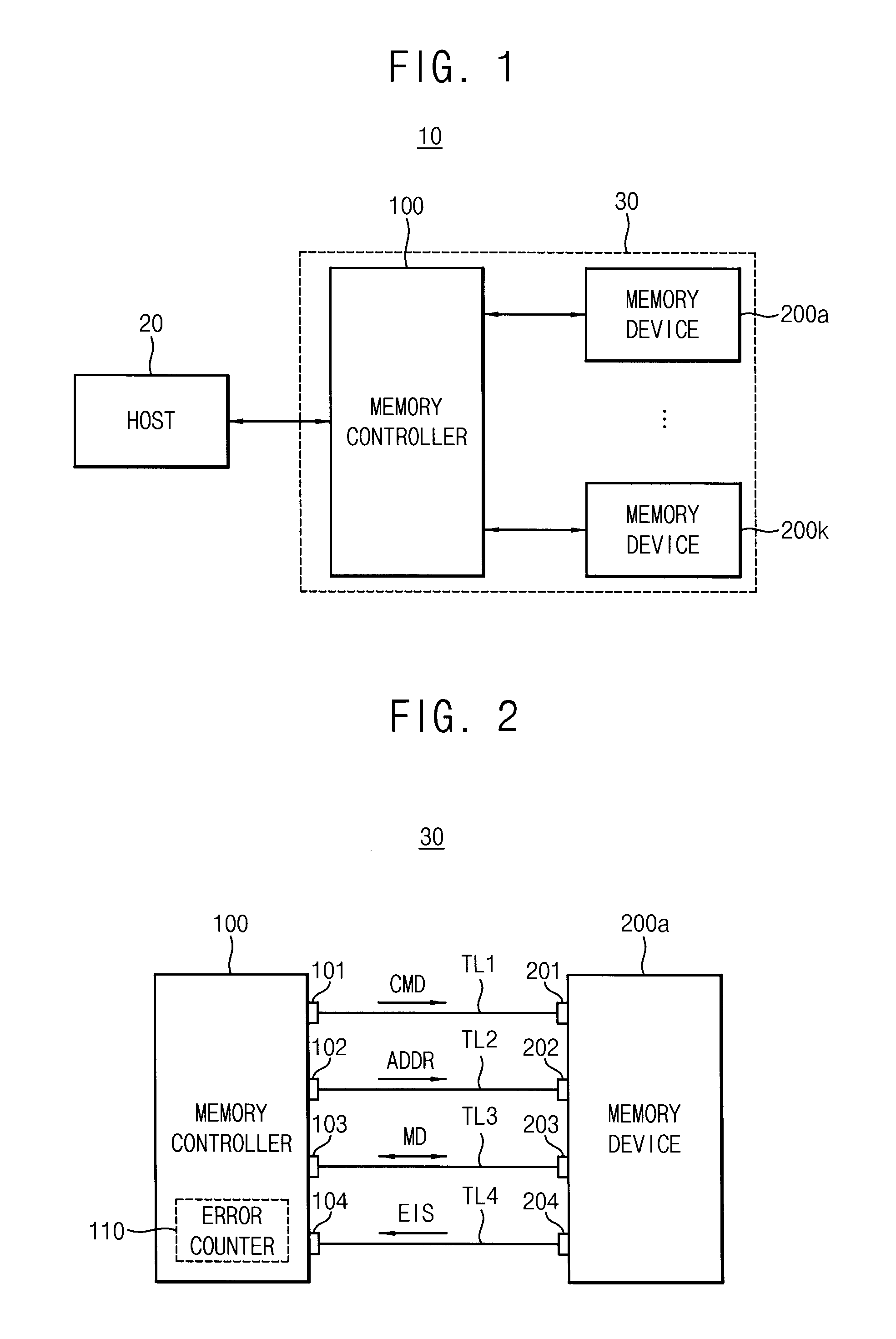
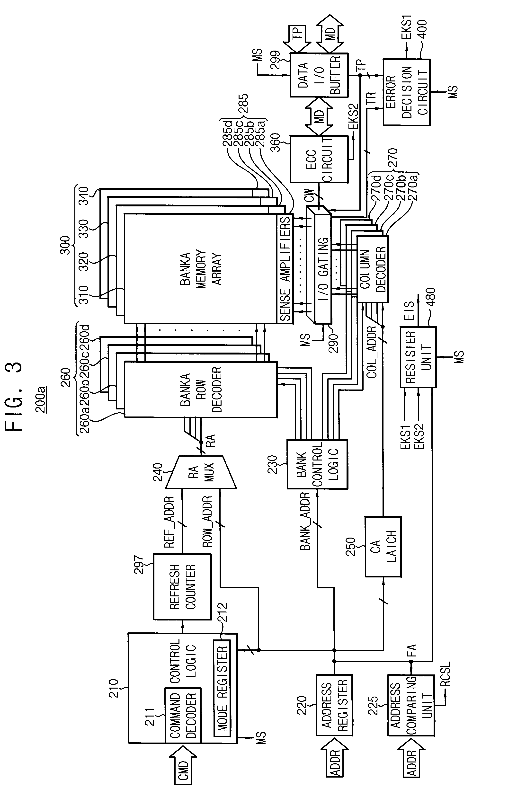
[0064]Various example embodiments will be described more fully hereinafter with reference to the accompanying drawings, in which some example embodiments are shown. The present disclosure may, however, be embodied in many different forms and should not be construed as limited to the example embodiments set forth herein. These example embodiments are just that—examples—and many implementations and variations are possible that do not require the details provided herein. It should also be emphasized that the present disclosure provides details of alternative examples, but such listing of alternatives is not exhaustive. Furthermore, any consistency of detail between various examples should not be interpreted as requiring such detail—it is impracticable to list every possible variation for every feature described herein. The language of the claims should be referenced in determining the requirements of the present disclosure. In the drawings, the sizes and relative sizes of layers and re...


PUM


Abstract

A semiconductor memory device includes a memory cell array, an input/output (I/O) gating circuit, an error decision circuit and an error check and correction (ECC) circuit. The I/O gating circuit reads test pattern data to provide test result data in a test mode and reads a codeword in a normal mode. The error decision circuit determines the correctability of errors in the test result data by a first unit, based on the test pattern data and the test result data and provides a first error kind signal indicating a first determination result, in the test mode. The ECC circuit decodes the codeword including main data and parity data generated based on the main, determines correctability of errors in the codeword by a second unit and provides a second error kind signal indicating a second determination result, in the normal mode. The main data includes a plurality of unit data.

Description

CROSS-REFERENCE TO RELATED APPLICATION(S)[0001]This U.S. non-provisional application claims the benefit of priority under 35 USC §119 to Korean Patent Application No. 10-2014-0103101, filed on Aug. 11, 2014, in the Korean Intellectual Property Office, the contents of which are incorporated herein in its entirety by reference.BACKGROUND[0002]1. Technical Field[0003]Example embodiments relate to memory devices, and more particularly to semiconductor memory devices and memory systems including the same.[0004]2. Discussion of the Related Art[0005]Semiconductor memory devices may be classified as non-volatile memory devices, such as flash memory devices, and volatile memory devices, such as Dynamic Random Access Memory devices (DRAMs). DRAMs are inexpensive and are used for storing mass data such as system memories. As the semiconductor fabrication process for volatile memory devices, such as DRAMs, continues to improve, thereby reducing the physical size of DRAMs, the bit error rate (BE...

Claims


Application Information

Patent Timeline
IPC IPC(8): G11C29/42G11C29/36G11C29/44
CPCG11C29/42G11C29/4401G11C29/36G11C11/401G11C29/44G11C29/52G11C2029/0411
Inventor KIM, YOUNG-ILCHUNG, HOI-JU
Owner SAMSUNG ELECTRONICS CO LTD
Why Eureka
Try Eureka