High voltage zero qrr bootstrap supply

a zero-qrr, high-voltage technology, applied in the direction of logic circuit coupling/interface arrangement, pulse generator, pulse technique, etc., can solve the problems of reducing the efficiency of high-voltage (100v) schottky diodes in the integrated circuit process, affecting the operation efficiency of high-frequency bootstraps, and reducing the losses induced in high-side devices. , the effect of high boot-strap supply voltag

Active Publication Date: 2016-04-14
EFFICIENT POWER CONVERSION CORP
View PDF1 Cites 28 Cited by
  • Summary
  • Abstract
  • Description
  • Claims
  • Application Information

AI Technical Summary

Benefits of technology

[0004]The present invention relates to a bootstrap supply for a half bridge topology, and, more particularly, a bootstrap supply using a gallium nitride (GaN) FET. Advantageously, a GaN FET is useful for high voltage applications because it has a zero reverse recovery charge QRR, and can be switched synchronously with the low side transistor of...

Problems solved by technology

However, it is very difficult to make a high voltage (100V) Schottky diode in an integrated circuit process and hence, PN junction diodes that have reverse recover charge are often used.
Moreover, high voltage Schottky diodes can also have reverse recovery charges (QRR) that lead to losses.
However, ...

Method used


Image

  • High voltage zero qrr bootstrap supply
  • High voltage zero qrr bootstrap supply
  • High voltage zero qrr bootstrap supply

Examples


Embodiment Construction

[0021]In the following detailed description, reference is made to exemplary embodiments of the present invention. The exemplary embodiments are described with sufficient detail to enable those skilled in the art to practice them. It is to be understood that other embodiments may be employed and that various structural, logical, and electrical changes may be made.

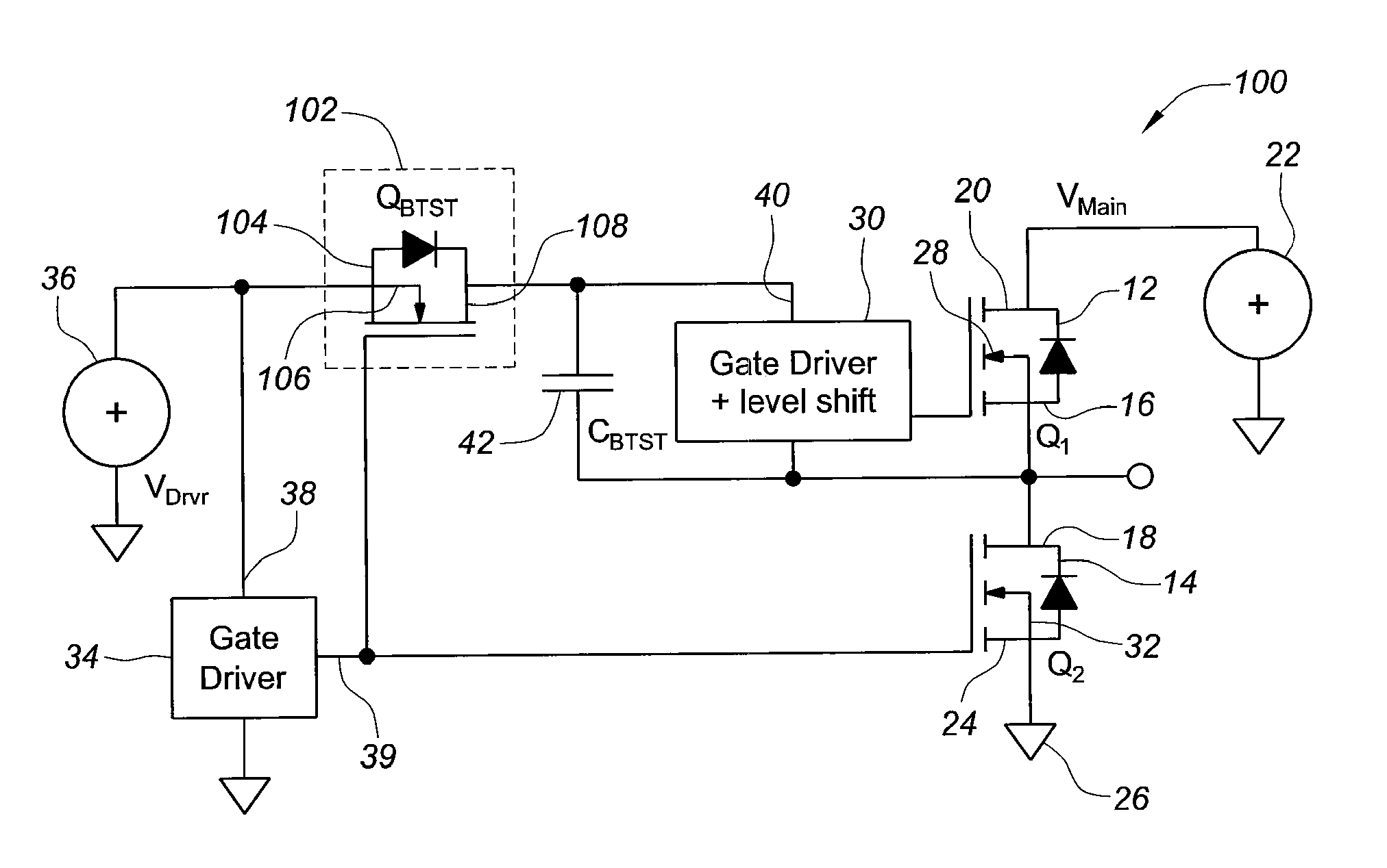
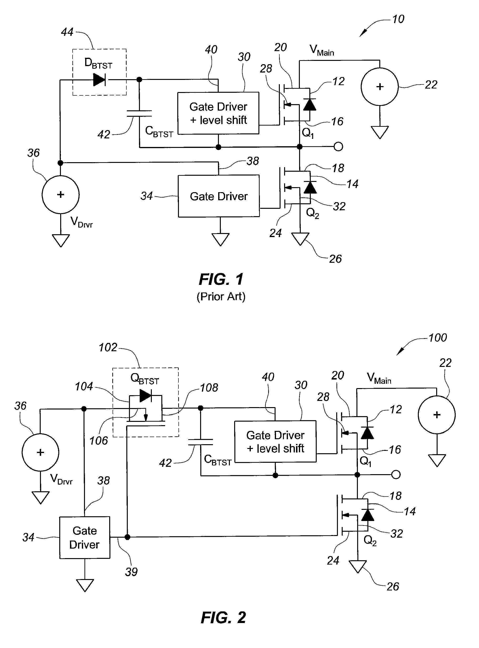
[0022]FIG. 2 illustrates a bootstrap supply for a half bridge topology according to a first embodiment 100 of the present invention. As shown, the design of FIG. 2 includes many of the same components as the conventional half bridge topology 10 discussed above. Namely, high side and low side transistors 12 and 14 (Q1 and Q2) are provided, with their respective gates coupled to a high side gate driver 34 and level shifter, and a low side gate driver 30, respectively. However, in contrast to the conventional design of FIG. 1, the exemplary design of FIG. 2 employs a depletion mode transistor (e.g., an n-channel depletion mode ...


PUM


Abstract

An electrical circuit arranged in a half bridge topology. The electrical circuit includes a high side transistor; a low side transistor; a gate driver and level shifter electrically coupled to a gate of the high side transistor; a gate driver electrically coupled to a gate of the low side transistor; a capacitor electrically coupled in parallel with the gate driver and level shifter; a voltage source electrically coupled to an input of the gate driver and level shifter and an input of the gate driver; and, a bootstrap transistor electrically coupled between the voltage source and the capacitor. A GaN field-effect transistor is synchronously switched with a low side device of the half bridge circuit.

Description

BACKGROUND OF THE INVENTION[0001]FIG. 1 illustrates a conventional half bridge topology 10. As shown, the conventional topology 10 includes a pair of transistors 12 and 14 labeled Q1 and Q2. Such a topology may, for example, be implemented with enhancement mode field effect transistors (FETs). Typically, the transistors 12 and 14 are considered high side and low side switches. The source 16 of high side transistor 12 is coupled to the drain 18 of low side transistor 14 at the half bridge output. The drain 20 of high side transistor 12 is coupled to a high voltage source 22 (VMAIN), and the source 24 of low side transistor 14 is coupled to ground 26. Furthermore, the gate 28 of high side transistor 12 is coupled to a gate driver and a level shifter 30 and the gate 32 of low side transistor 14 is coupled to a gate driver 34. Gate drivers 30 / 34 and level shifters 30 are well-known in the art and will not be described in detail herein. However, it should be understood that this configur...

Claims


Application Information

Patent Timeline
IPC IPC(8): H03K17/687
CPCH03K17/6871H03K17/04206H03K17/165H03K2217/0081H03K19/017509H03K2217/0063H03K2217/0072H03K17/567
Inventor DE ROOIJ, MICHAEL A.STRYDOM, JOHAN T.REUSCH, DAVID C.
Owner EFFICIENT POWER CONVERSION CORP
Why Eureka
Try Eureka