Surface-treated copper foil, copper foil with carrier, substrate, resin substrate, printed wiring board, copper clad laminate and method for producing printed wiring board

a technology of printed wiring and copper clad laminate, which is applied in the direction of textiles and paper, metal pattern materials, and recording information storage, etc., can solve the problems of difficult to form fine circuits on the basis of subtractive methods, and achieve satisfactory electroless adhesion and maintain fine wiring formability.

Active Publication Date: 2016-06-23
JX NIPPON MINING & METALS CO LTD
View PDF2 Cites 27 Cited by
  • Summary
  • Abstract
  • Description
  • Claims
  • Application Information

AI Technical Summary

Benefits of technology

[0173]According to the present invention, it is possible to provide a surface-treated copper foil capable of imparting a profile shape of the substrate surface after removal of the copper foil, capable of maintaining fine wiring formability and implementing satisfactory adhesion of electroless copper plating coating, and a resin substrate provided with the profile shape of the surface.

Problems solved by technology

However, recently, due to high integration of semiconductors, miniaturization has been advanced in the circuits of semiconductor package substrates and printed wiring boards used for highly integrated semiconductors, and accordingly it has been becoming difficult to form fine circuits on the basis of subtractive methods.

Method used


Image

  • Surface-treated copper foil, copper foil with carrier, substrate, resin substrate, printed wiring board, copper clad laminate and method for producing printed wiring board
  • Surface-treated copper foil, copper foil with carrier, substrate, resin substrate, printed wiring board, copper clad laminate and method for producing printed wiring board
  • Surface-treated copper foil, copper foil with carrier, substrate, resin substrate, printed wiring board, copper clad laminate and method for producing printed wiring board

Examples


examples

[0459]Hereinafter, Examples of the present invention are described; these Examples are presented for the purpose of better understanding of the present invention and the advantages thereof, and are not intended to limit the present invention.

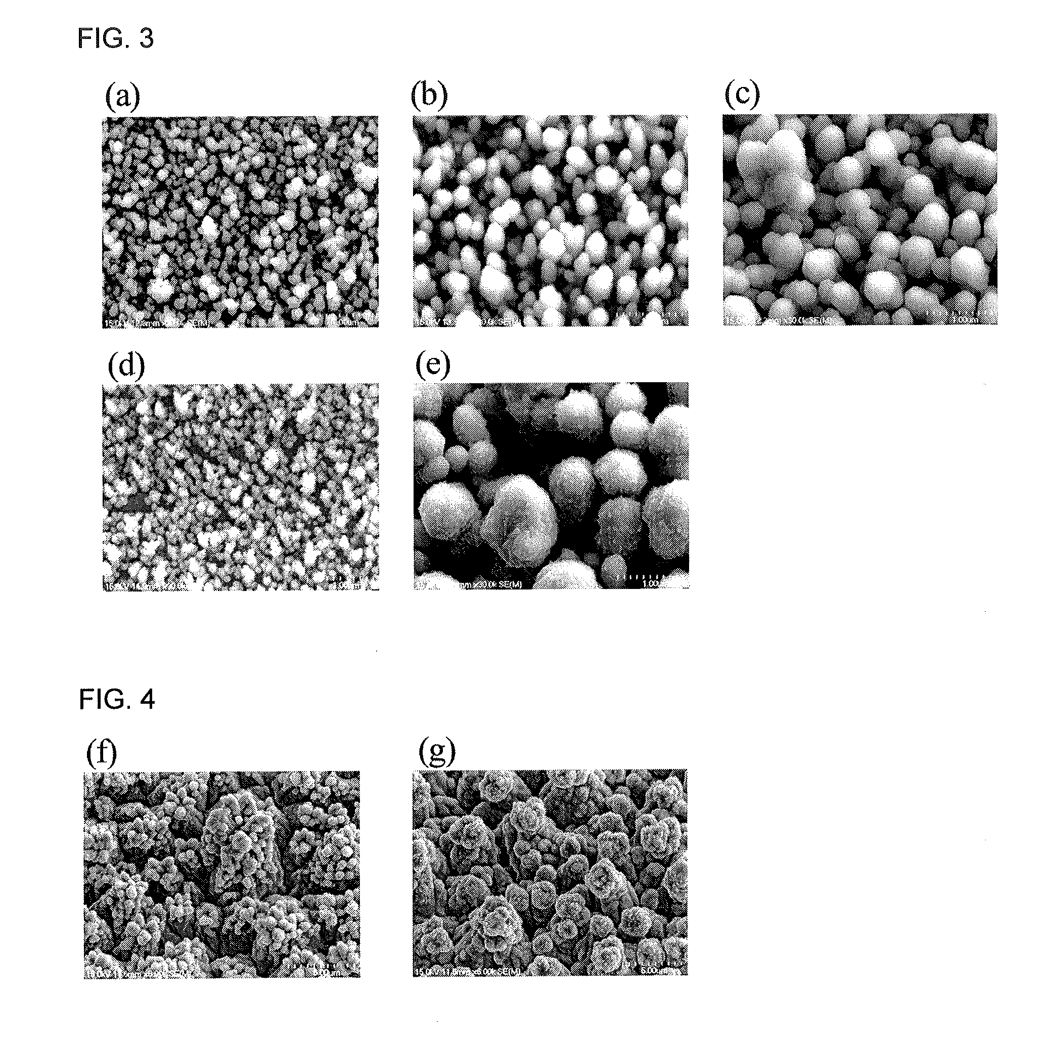
[0460]In present Example, as described below, the surface profile of the resin substrate formed by using a copper foil and the surface profile of the resin substrate formed by using a chemical solution were produced.

[0461]1. Formation of Surface Profile of Resin Substrate Using Copper Foil

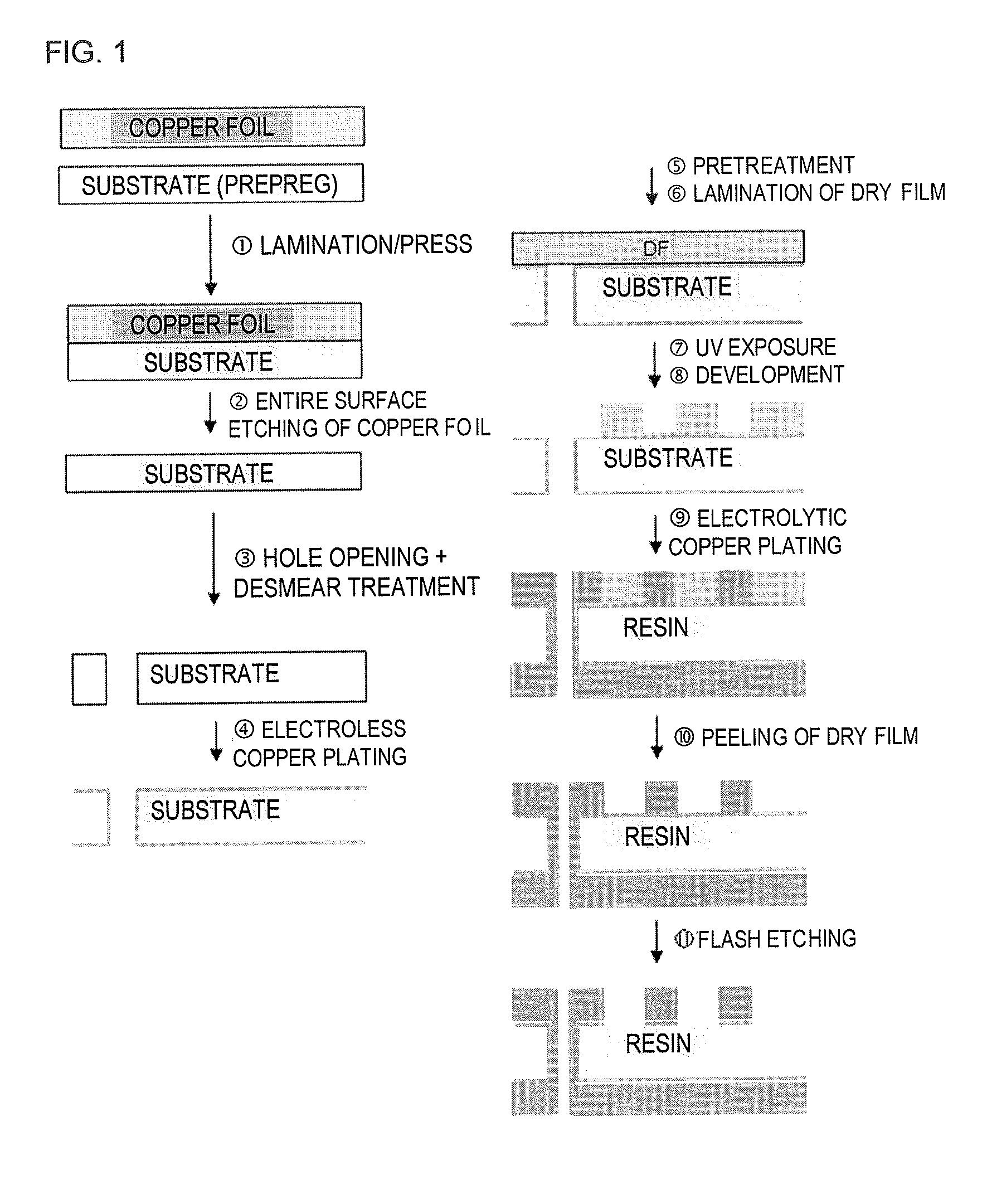
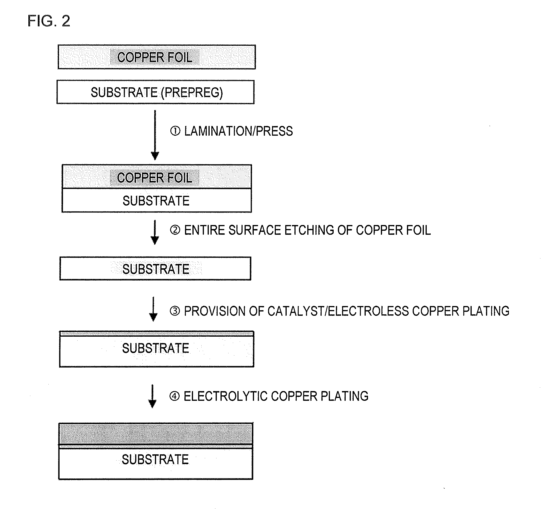
[0462]FIG. 2 illustrates a production flow of samples for obtaining the data of Examples and Comparative Examples.

[0463]As Examples A1 to A11 and Comparative Examples A1 to A4, and as the copper foils for producing the substrate surface profiles of Examples B1 to B8, Examples B10 to B12 and Comparative Examples B1 to B4, the following copper foil bulk layers (raw foils) were prepared.

[0464]Common Electrolytic Raw Foil

[0465]A copper sulfate electrolyte having a ...


PUM


Abstract

The present invention provides a surface-treated copper foil capable of imparting the profile shape of the substrate surface after removal of the copper foil, the profile shape maintaining fine wiring formability and achieving satisfactory adhesion of electroless copper plating coating. The present invention also provides a resin substrate provided with a profile shape of the surface maintaining fine wiring formability and achieving satisfactory adhesion of electroless copper plating coating. The surface-treated copper foil of the present invention is a surface-treated copper foil having a surface-treated layer formed on a copper foil, and the surface roughness Sz of the surface of the surface-treated layer is 2 to 6 μm.

Description

TECHNICAL FIELD[0001]The present invention relates to a surface-treated copper foil, a copper foil with carrier, a substrate, a resin substrate, a printed wiring board, a copper clad laminate and a method for producing a printed wiring board.[0002]As the method for forming circuits of a semiconductor package substrate and a printed wiring board, a subtractive method is predominantly used. However, recently, due to high integration of semiconductors, miniaturization has been advanced in the circuits of semiconductor package substrates and printed wiring boards used for highly integrated semiconductors, and accordingly it has been becoming difficult to form fine circuits on the basis of subtractive methods.[0003]As measures for forming further finer wirings, the following methods have been attracting attention: a circuit forming method (1) in which pattern copper plating is performed by using an ultra-thin copper foil as a power feeding layer, and finally the ultra-thin copper layer i...

Claims


Application Information

Patent Timeline
Patent Type & Authority Applications(United States)
IPC IPC(8): H05K3/02H05K3/38B32B15/08H05K3/20
CPCH05K3/025H05K3/205H05K3/384B32B2457/08B32B15/08H05K2203/072H05K2203/0726H05K3/389B32B15/20B32B3/26C25D7/0614C25D7/0671C23C18/1653H05K1/09H05K3/388H05K2201/0355H05K2203/0307H05K3/427H05K2203/1152C25D1/04C25D3/38C25D3/562C25D3/58C25D5/022C25D5/10C25D5/18C25D5/34C25D5/48C23C18/405C25D5/611
Inventor ISHII, MASAFUMIHONDA, MISATOMIYAMOTO, NOBUAKI
Owner JX NIPPON MINING & METALS CO LTD
Why Eureka
Try Eureka