
Image forming apparatus

Inactive Publication Date: 2016-06-30
CANON KK
View PDF14 Cites 6 Cited by
  • Summary
  • Abstract
  • Description
  • Claims
  • Application Information

AI Technical Summary

Benefits of technology

This patent aims to reduce noise in an image forming apparatus with multiple image forming units. The invention causes noise in different units to not overlap, resulting in a quieter output.

Problems solved by technology

However, because the class-D amplifier performs switching driving of a bridge circuit at a high frequency, a radiation noise occurs, and because a ferrite bead or a filter is used as a noise counter-measure, this leads to a cost increase.
For this reason, there is the problem that the frequencies of the PWM signals of the class-D amplifiers used corresponding to respective color photosensitive drums overlap, and radiation noise worsens.

Method used


Image

  • Image forming apparatus
  • Image forming apparatus
  • Image forming apparatus

Examples


first embodiment

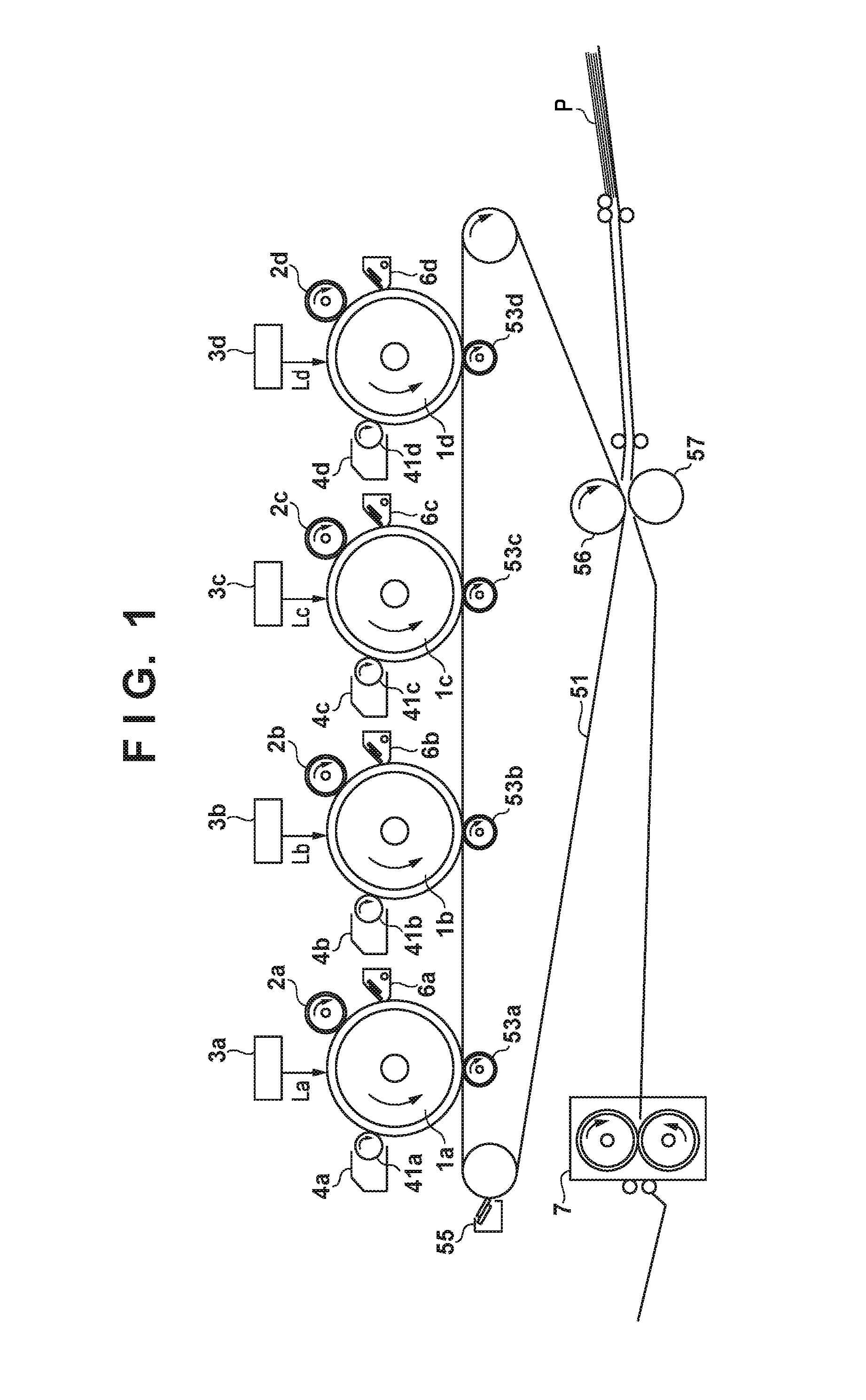
[0039]FIG. 1 depicts a view for explaining a configuration of an image forming unit of a color image forming apparatus according to a first embodiment of the present invention.

[0040]This color image forming apparatus is an image forming apparatus for forming an image using a electrophotographic process comprising a high-voltage power supply circuit for charging. This color image forming apparatus comprises of four image forming units (stations) of yellow, magenta, cyan, and black. In the figure, a to d added after reference numerals correspond to each image forming unit from yellow, magenta, cyan, and black. Explanation is given omitting a to d in the explanation of FIG. 1. A charging roller 2, a developing unit 4, a cleaner 6, and a primary transfer roller 53 are arranged in a periphery of a drum of a photoconductive member 1. An exposure unit 3 generates a laser beam in accordance with image data of each color and irradiates a surface of each corresponding photoconductive member 1...

second embodiment

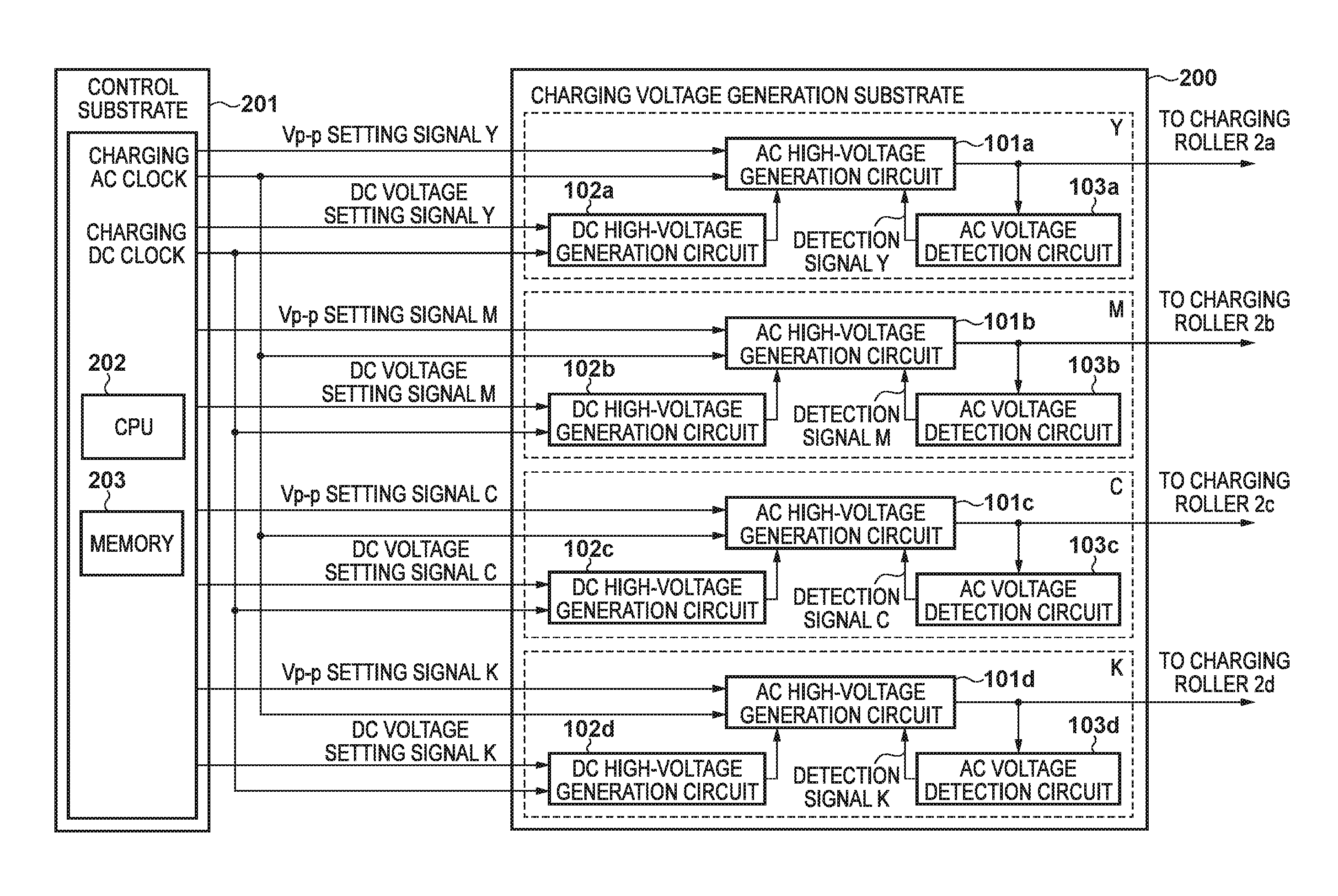
[0086]In the previously described first embodiment, explanation is given for an example of a high-voltage circuit for charging of an electrophotographic image forming apparatus, but in the second embodiment explanation is given an example using a high-voltage circuit that generates a developing voltage. Note that because the basic configuration of the image forming apparatus according to a second embodiment is the same as in the first embodiment, detailed explanation is given for portions that differ to the first embodiment.

[0087]FIG. 14 is a block diagram for describing an overview configuration of a developing voltage generation substrate 1401 and the control substrate 201 of the color image forming apparatus according to a second embodiment of the present invention.

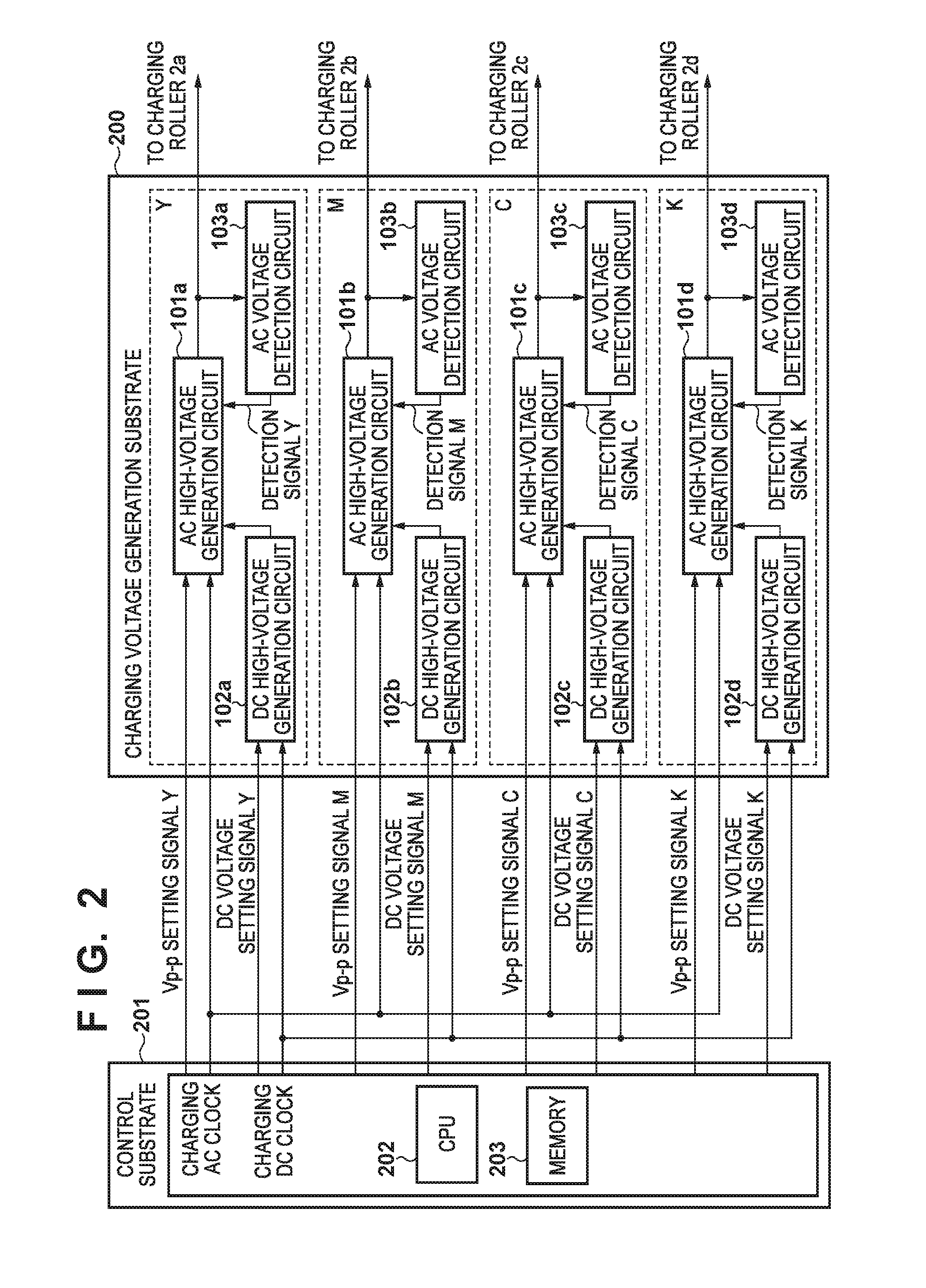
[0088]The control substrate 201 includes a CPU 202 responsible for controlling the entirety of this color image forming apparatus and a memory 203 for storing programs, similarly to in the case of the first embodiment....

third embodiment

[0120]Next, explanation will be given for a third embodiment of the present invention. In the third embodiment, the frequencies of the PWM signals are made to be modifiable when image forming and when in a standby state waiting for image forming. Here, the embodiment is for a case in which with respect to the frequency adjustment resistor R1 connected to the oscillation circuit 411 according to the first embodiment, another frequency adjustment resistor R2 is connected in parallel, and basic configuration is the same as in the first embodiment.

[0121]FIG. 20 is a block diagram for illustrating a configuration of the class-D amplifier according to the third embodiment. In FIG. 20, portion common to previously described FIG. 4 are indicated by the same reference numerals. A class-D amplifier 2001 is included in the AC high-voltage generation circuit 101a of FIG. 2.

[0122]The class-D amplifier 2001 has a full bridge circuit including the oscillation circuit 411, the triangle wave generat...


PUM


Abstract

An image forming apparatus comprises a plurality of image forming units that respectively form an image, and a plurality of voltage generation circuits that respectively generate voltages for driving the plurality of image forming units. Each of the plurality of voltage generation circuits comprises a voltage generation circuit having a transformer, and generates a voltage by a switching operation that is driven by changing an input voltage of primary side of the transformer, an oscillation circuit that generates a clock signal of a frequency that becomes a reference frequency of the switching operation and a setting unit that sets the frequency of the clock signal that the oscillation circuit generates. The setting units of the plurality of voltage generation circuits set the frequencies of the respective clock signals.

Description

BACKGROUND OF THE INVENTION[0001]1. Field of the Invention[0002]The present invention relates to an image forming apparatus.[0003]2. Description of the Related Art[0004]In an electrophotographic image forming apparatus, charging of a surface of a photosensitive drum is performed uniformly by a charger, and the charged surface of the photosensitive drum is exposed by a laser beam which is modulated in accordance with image data and irradiated by an exposure unit, thereby forming an electrostatic latent image. Then, by a developer (hereinafter referred to as a toner) supplied from a developing unit, the electrostatic latent image is developed and a toner image is thereby formed.[0005]For photosensitive drum surface charge processing, an AC charging scheme that charges by causing a charging roller to abut the surface of the photosensitive drum, for example, applying a voltage that overlaps a direct current voltage and an alternating voltage to the charging roller, and discharging to th...

Claims


Application Information

Patent Timeline
IPC IPC(8): G03G15/00
CPCG03G15/0266G03G15/0189G03G15/80
Inventor KAGAWA, YOSUKE
Owner CANON KK
Learn More