Semiconductor device

a technology of semiconductor modules and inductance, which is applied in the direction of hermetically sealed casings, electrical apparatus casings/cabinets/drawers, and semiconductor/solid-state device details. it can solve the problems of increasing the size of power semiconductor modules, reducing the current-carrying capacity, and reducing the inductance of wiring. reduce the effect of wiring inductance and increasing the current-carrying capacity

Active Publication Date: 2016-06-30
FUJI ELECTRIC CO LTD
View PDF3 Cites 27 Cited by
  • Summary
  • Abstract
  • Description
  • Claims
  • Application Information

AI Technical Summary

Benefits of technology

[0012]Using the technology disclosed here, the inductance of the wiring can be reduced while increasing the current-carrying capacity. It is to be understood that both the foregoing general description and the following detailed description are exemplary and explanatory, and are intended to provide further explanation of the invention as claimed.

Problems solved by technology

Although the amount of current that flows out in this way is large, because the current path between where the current goes in and out is long, restraining the inductance of the wiring is difficult.
Thus, increasing the size of the power semiconductor module is unavoidable.
Furthermore, because the current path would be longer in a larger module, restraining the inductance of the wiring becomes even more difficult.

Method used


Image

  • Semiconductor device
  • Semiconductor device
  • Semiconductor device

Examples


embodiment 1

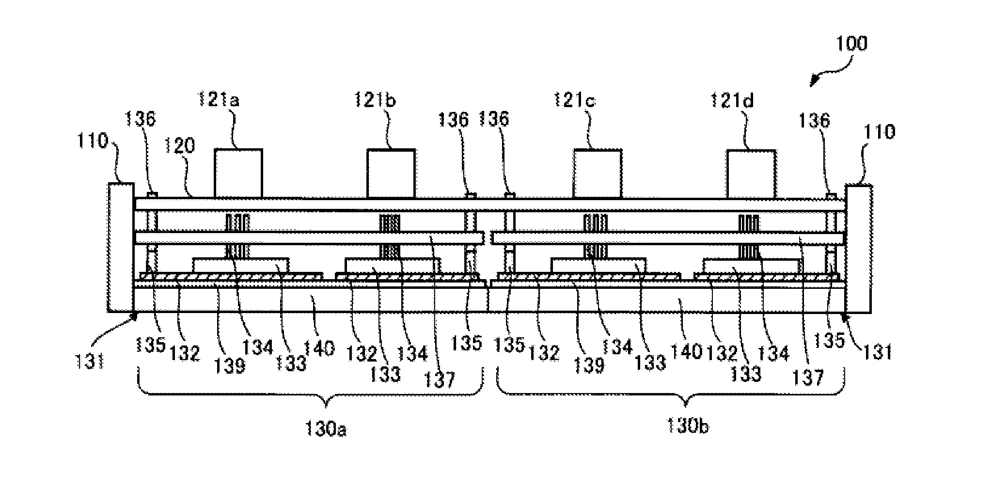
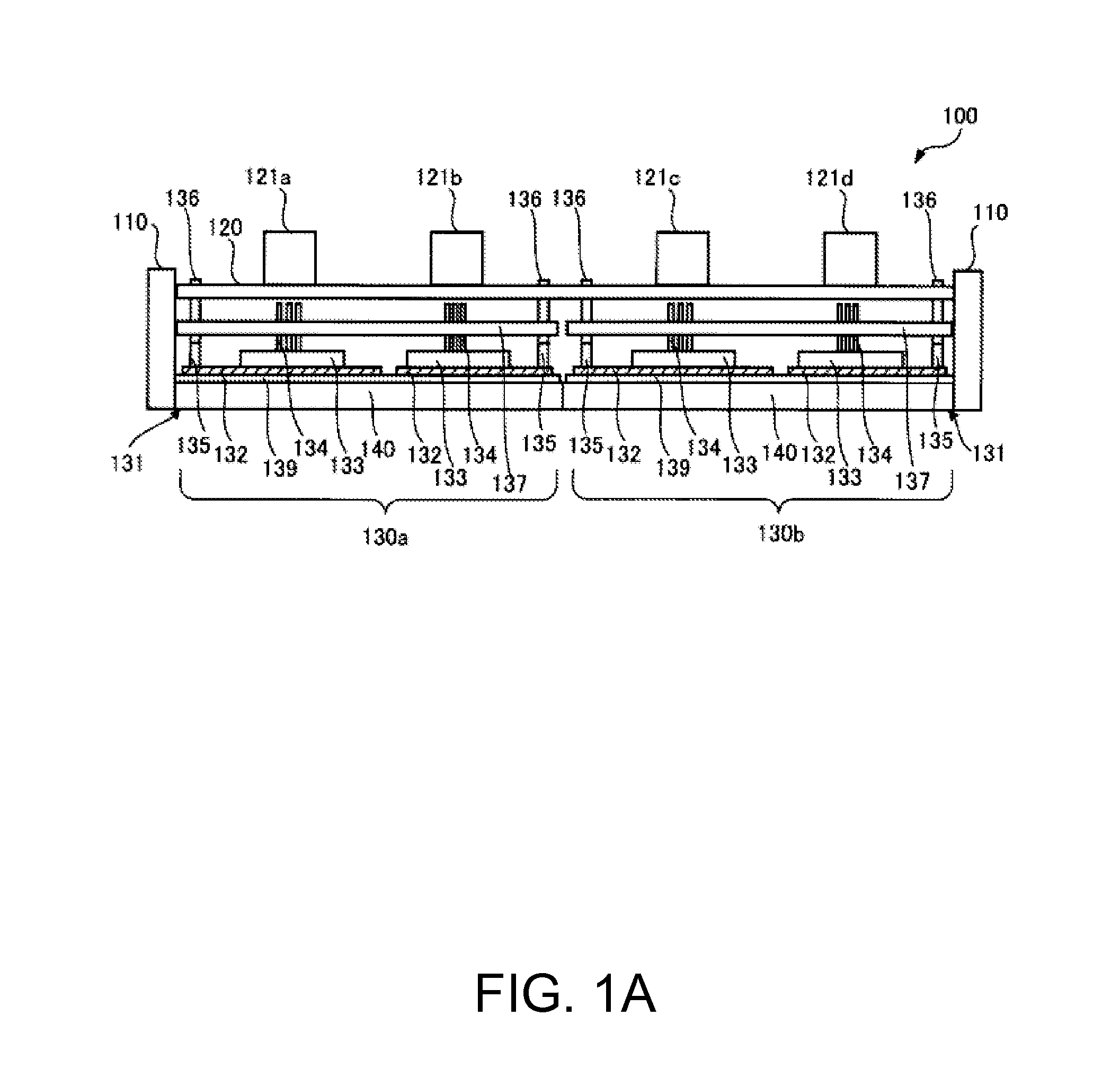
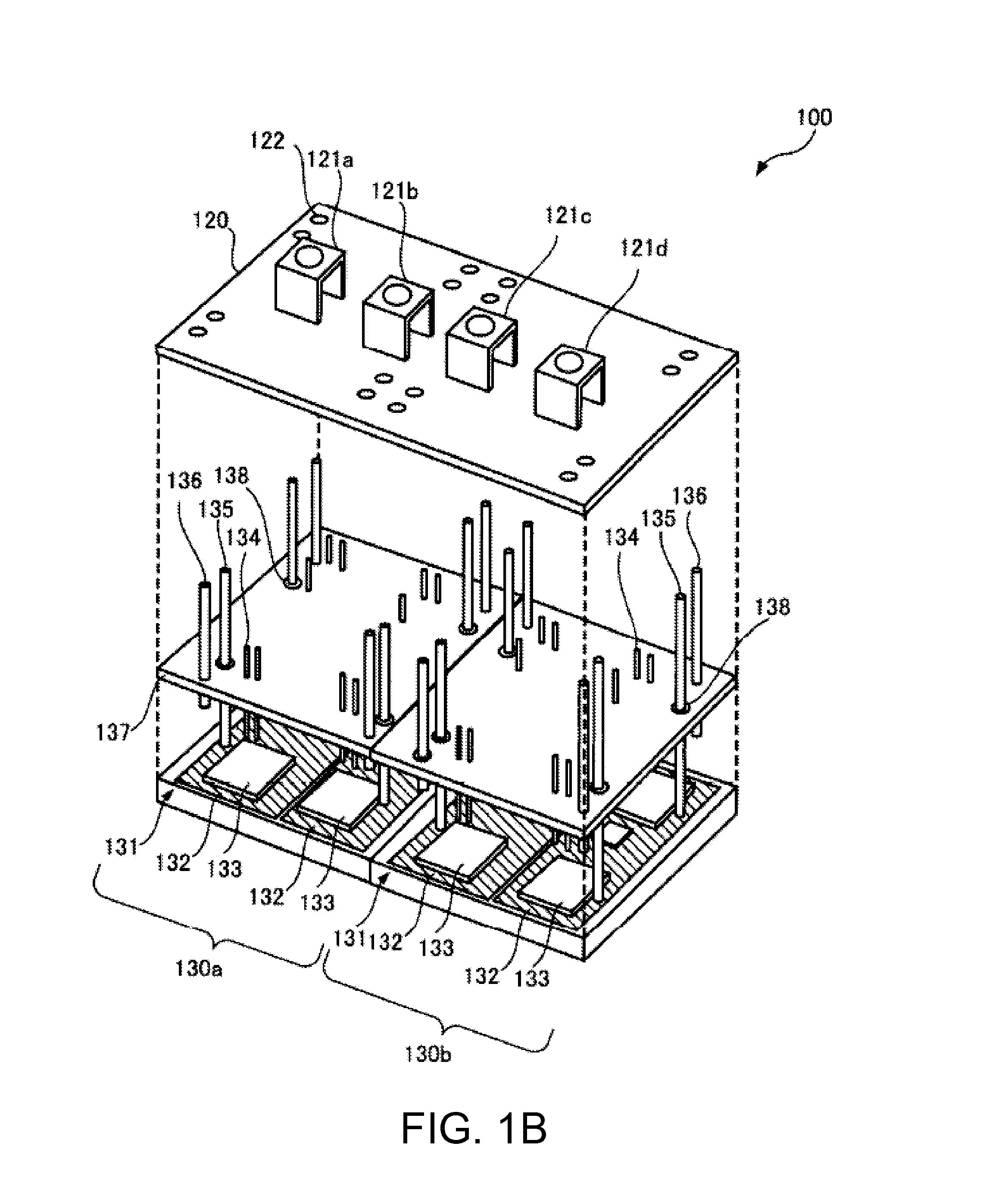
[0029]FIGS. 1A and 1B are views used to describe a semiconductor device according to Embodiment 1. FIG. 1A is a cross-sectional view of a semiconductor device. FIG. 1B is an exploded perspective view of the semiconductor device. In FIG. 1B, a case is not shown. As shown in FIGS. 1A and 1B, a semiconductor device 100 equipped with a three-level inverter circuit includes a plurality (two) of semiconductor units 130a and 130b and a connection unit 120 electrically connecting the semiconductor units 130a and 130b in parallel. The semiconductor device 100 further includes a case 110.

[0030]Embodiment 1 describes an example in which a printed circuit board is used for the connection unit 120. The connection unit 120 is formed by stacking a plurality of circuit layers (not shown) inside. On the connection unit 120, there are external terminals 121a to 121d connected to respective circuit layers. The external terminals 121a to 121d correspond respectively to a P terminal, an M terminal, an N...

embodiment 2

[0046]A semiconductor device according to Embodiment 2 is described using FIGS. 2A to 8. FIGS. 2A and 2B are views showing a semiconductor device according to Embodiment 2. FIG. 2A is a top view of a semiconductor device, and FIG. 2B is a cross-sectional view of FIG. 2A along one-dot-chain line X-X.

[0047]FIG. 3 is a perspective view showing semiconductor units and a connection unit equipped in a semiconductor device according to Embodiment 2. In FIG. 3, a case is not shown. A semiconductor device 1000 includes four semiconductor units 1300a to 1300d and a connection unit 1200 that electrically connects each of the semiconductor units 1300a to 1300d in parallel. Furthermore, the semiconductor device 1000 includes a case 1100 that houses the semiconductor units 1300a to 1300d.

[0048]In the central region, the case 1100 can house the semiconductor units 1300a to 1300d in two rows and two columns. Although an example in which the four semiconductor units 1300a-1300d are housed in two ro...

embodiment 3

[0098]Embodiments 1 and 2 described an example in which wiring members for semiconductor elements and diodes inside a semiconductor unit (hereafter these components may be collectively referred to as a “semiconductor chip”) included a plurality of conductive posts and a printed circuit board. Embodiment 3 describes, using FIG. 9, a case in which wiring members for a semiconductor chip inside a semiconductor unit placed on a multi-layer substrate include a plurality of wires.

[0099]FIG. 9 is a view showing a multi-layer substrate when wiring members according to Embodiment 3 include a plurality of wires. A multi-layer substrate 2330 has the same configuration as a multi-layer substrate 1330 according to Embodiment 2. Specifically, the multi-layer substrate 2330 includes an insulating plate 1331 made of material such as ceramic, circuit plates 1332a to 1332d, and circuit plates 1332e to 1332l. The circuit plates 1332a to 1332l are disposed on the primary surface (the front surface) of ...


PUM


Abstract

A semiconductor device including: a plurality of semiconductor units each constituting a three-level inverter circuit; and a connection unit electrically connecting the plurality of semiconductor units in parallel, wherein each of the semiconductor units includes: a multi-layer substrate including an insulating plate and circuit plates disposed on a primary surface of the insulating plate; a plurality of semiconductor elements each having a back surface thereof fixed to one of the circuit plates and a front surface thereof having primary electrodes; and wiring members electrically connected to the primary electrodes of the semiconductor elements, and wherein in each of the semiconductor units, the multi-layer substrate, the plurality of semiconductor elements, and the wiring members are configured in such a way as to constitute the three-level inverter circuit.

Description

BACKGROUND OF THE INVENTION[0001]1. Technical Field[0002]The present invention relates to a semiconductor device.[0003]2. Background Art[0004]A semiconductor device called a power semiconductor module includes a semiconductor chip, on which semiconductor elements such as IGBTs (Insulated Gate Bipolar Transistor) or FWDs (Free Wheeling Diode) are formed, and is widely used as a power converter.[0005]In recent years, a power semiconductor module equipped with a three-level inverter circuit is being used in fields that seek to improve technologies such as wind power generation and solar power generation (refer to Patent Document 1, for example).RELATED ART DOCUMENTPatent Document[0006]Patent Document 1: Japanese Patent Application Laid-Open Publication No. 2012-110095SUMMARY OF THE INVENTION[0007]In the power semiconductor module described in Patent Document 1, when a voltage is applied from a connection terminal, a current flows through elements in the module and a conductive layer fo...

Claims


Application Information

Patent Timeline
Patent Type & Authority Applications(United States)
IPC IPC(8): H05K1/18H05K7/14H05K1/11H02M7/44H01L23/522H05K5/06H02M7/487
CPCH05K1/181H01L23/5227H05K7/1427H05K1/11H02M7/44H05K5/064H01L25/072H02M7/003H01L2225/04H02M7/487H05K1/0265H05K1/145H05K2201/10166H05K2201/10295H01L23/3735H01L23/49811H01L23/5385H01L2924/0002H01L2224/0603H01L2224/48139H01L2224/49113H01L2224/49111H01L2224/4846H05K7/14329H05K7/1432
Inventor NAKAMURA, HIDEYOYAMADA, RYUJITAKUBO, HIROMU
Owner FUJI ELECTRIC CO LTD
Why Eureka
Try Eureka