Method for producing a semiconductor device

a technology of nitride and semiconductor layer, which is applied in the manufacture of semiconductor/solid-state devices, semiconductor devices, electrical equipment, etc., can solve the problems of insufficient crystallization of izo, and achieve the effects of reducing light absorption due to strain, improving translucency and conductivity, and reducing strain between transparent electrode and semiconductor layer

Active Publication Date: 2016-07-21
TOYODA GOSEI CO LTD
View PDF0 Cites 1 Cited by
  • Summary
  • Abstract
  • Description
  • Claims
  • Application Information

AI Technical Summary

Benefits of technology

[0016]According to the present invention, a strain between the transparent electrode and the semiconductor layer can be reduced. Particularly in the light-emitting device, light absorption due to a strain can be reduced. Moreover, translucency and conductivity can be improved by further promoting the crystallization of the transparent electrode, thereby improving the emission efficiency.

Problems solved by technology

IZO could not be sufficiently crystallized when p-activation and crystallization of the transparent electrode are performed at the same time because a temperature suitable for crystallization of IZO is high.

Method used


Image

  • Method for producing a semiconductor device
  • Method for producing a semiconductor device
  • Method for producing a semiconductor device

Examples


embodiment 1

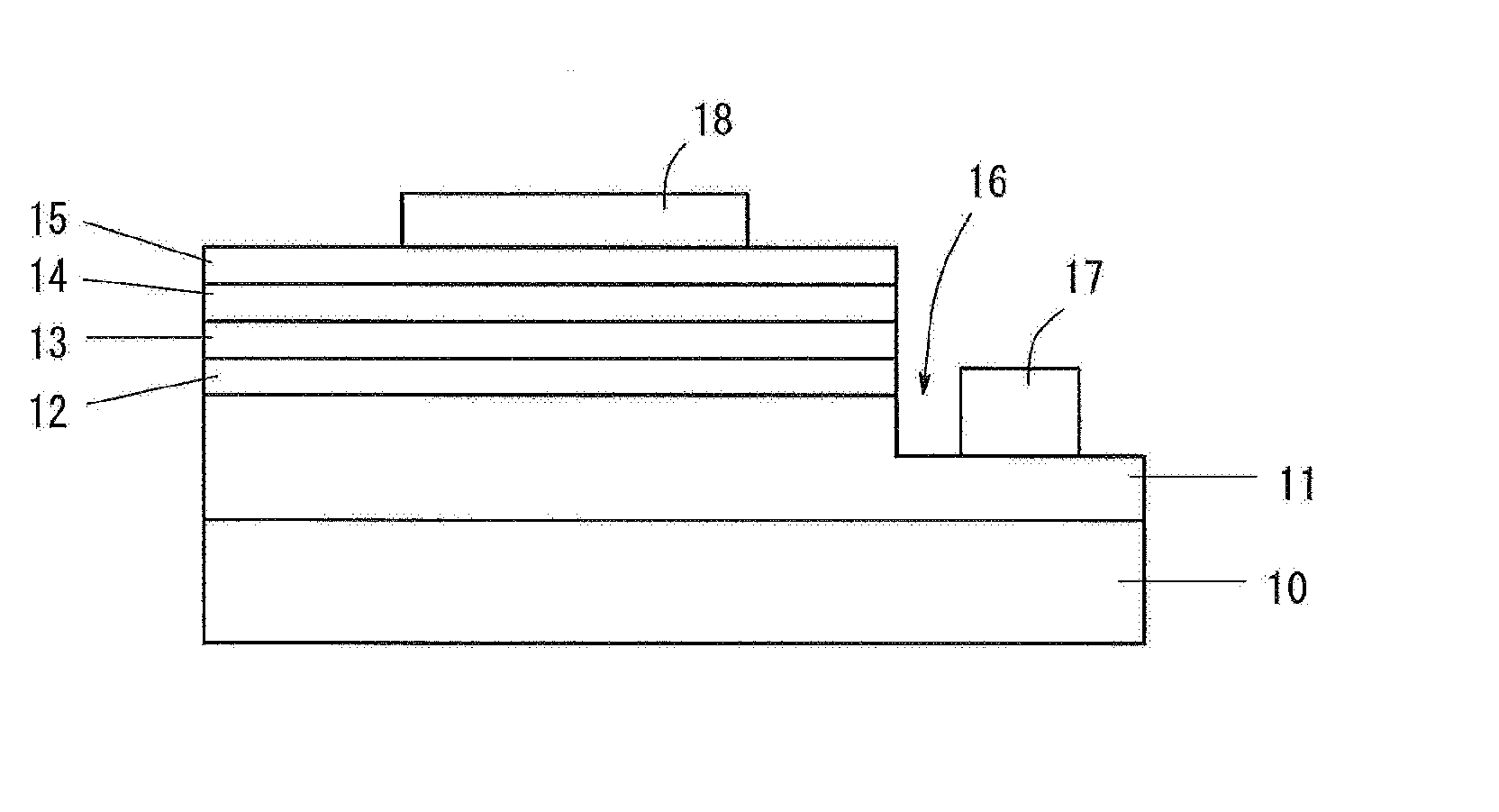
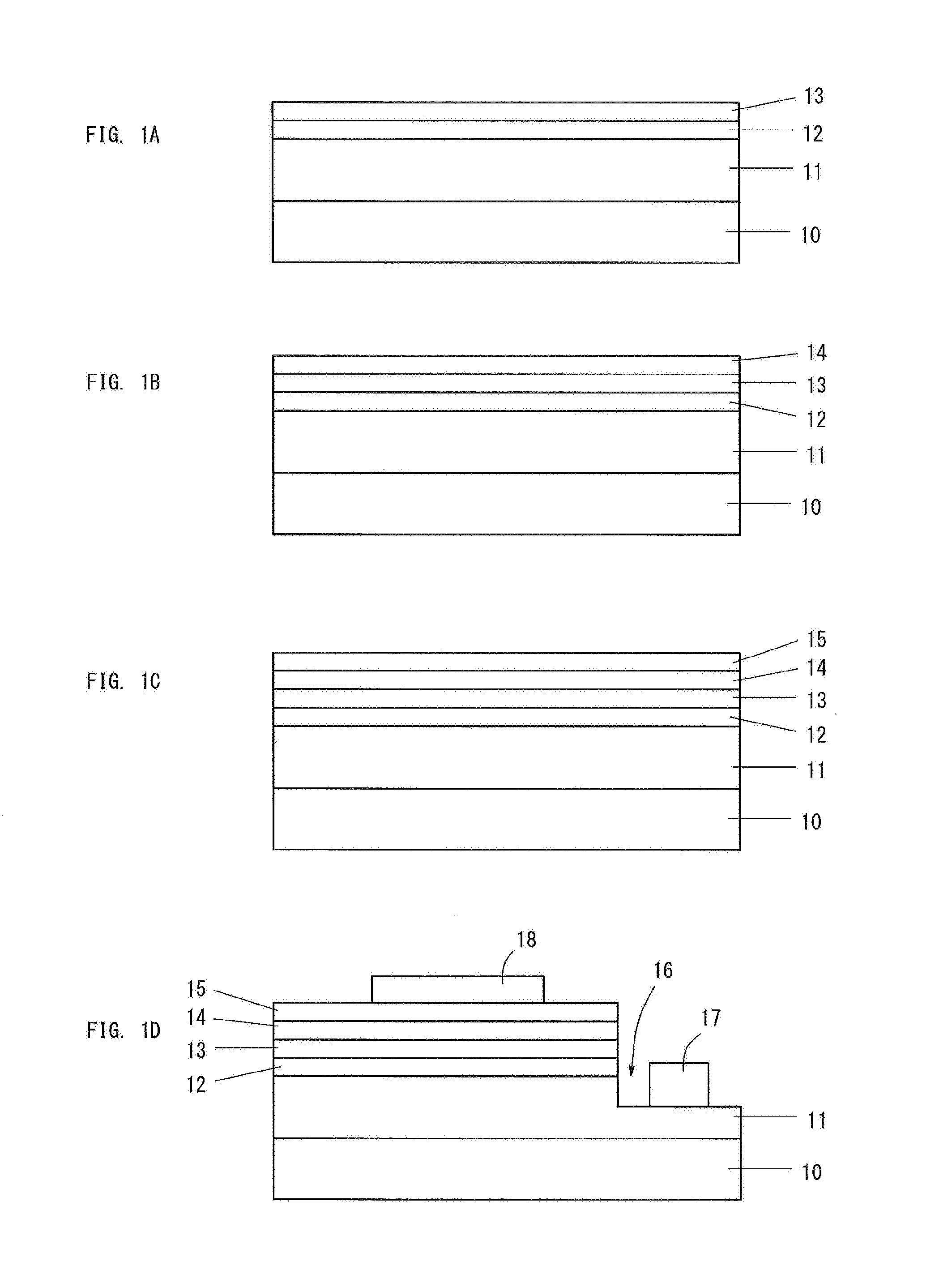
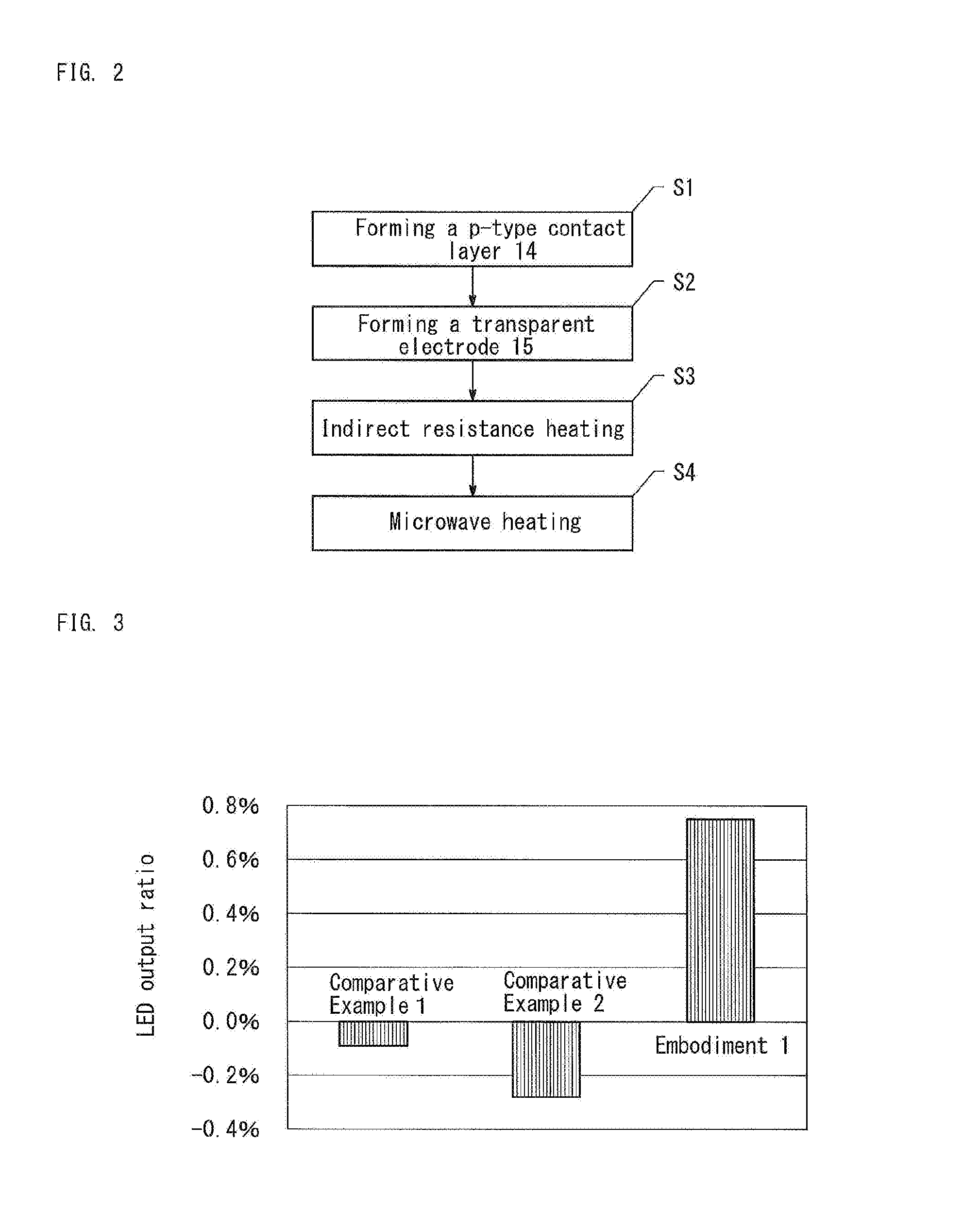
[0025]FIGS. 1A to 1D are sketches showing processes for forming a light-emitting device according to Embodiment 1. FIG. 2 is a flowchart showing a part (before and after the formation of transparent electrode 15) of the processes for producing a light-emitting device according to Embodiment 1. Next will be described the processes for producing the Group III nitride semiconductor light-emitting device according to Embodiment 1 with reference to FIGS. 1A to 1D, and FIG. 2.

[0026]Firstly, a sapphire substrate 10 was prepared, and thermally treated in a hydrogen atmosphere so as to remove impurities adhering to the surface. Next, an AlN buffer layer (not illustrated) was formed on the sapphire substrate 10. An n-type layer 11, a light-emitting layer 12, and a p-type cladding layer 13 were sequentially deposited through MOCVD on the buffer layer (FIG. 1A).

[0027]Each of the n-type layer 11, the light-emitting layer 12, and the p-type cladding layer 13 may have various known structures.

[002...


PUM

PropertyMeasurementUnit
temperatureaaaaaaaaaa

Abstract

The present invention provides a method for producing a semiconductor device exhibiting the improved emission efficiency by reducing a strain between a p-contact layer and a transparent electrode. A transparent electrode made of IZO (Zinc-doped Indium Oxide) was formed on a p-type contact layer by vapor deposition or sputtering. Subsequently, a p-type cladding layer and a p-type contact layer were p-type activated and a transparent electrode was crystallized by indirect resistance heating. This heat treatment was performed under a reduced pressure at a temperature of 700° C. Next, microwave heating was performed for three to thirty minutes at a temperature of 100° C. to 350° C. by microwave irradiation with a frequency of 5.8 GHz in a nitrogen atmosphere. This reduced a strain of the transparent electrode, and improved the conductivity or translucency of the transparent electrode.

Description

BACKGROUND OF THE INVENTION[0001]1. Field of the Invention[0002]The present invention relates to a method for producing a Group III nitride semiconductor device, and more specifically, to a method for reducing a strain between a Group III nitride semiconductor and a transparent electrode.[0003]2. Background Art[0004]In the conventional method for producing a Group III nitride semiconductor light-emitting device, after the formation of the transparent electrode made of a material such as ITO and IZO on a p-type layer, heat treatment is performed to crystallize the transparent electrode. This improves the conductivity of the transparent electrode and reduces the light absorptivity.[0005]Japanese Patent Application Laid-Open (kokai) No. 2014-154584 describes that the p-type layer and the transparent electrode are preferentially heated by microwave heating so as to activate the p-type layer and crystallize the transparent electrode at the same time.[0006]However, as crystallization of t...

Claims


Application Information

Patent Timeline
Patent Type & Authority Applications(United States)
IPC IPC(8): H01L33/42H01L33/00H01L33/32
CPCH01L33/42H01L2933/0016H01L33/0095H01L33/32
Inventor TOTANI, SHINGONAKAUCHI, JUN
Owner TOYODA GOSEI CO LTD
Why Eureka
Try Eureka