Multilayer ceramic capacitor, mounting structure of multilayer ceramic capacitor, and taped electronic component array

a multi-layer ceramic and capacitor technology, applied in the direction of printed circuit non-printed electric components association, sustainable manufacturing/processing, final product manufacturing, etc., can solve the problems of difficult to ensure moisture resistance, peeling may occur in the interface between the internal electrode and the dielectric ceramic layer, etc., to achieve the effect of reducing the connection resistance between the external electrode and the internal electrode, improving the connection efficiency and improving the high frequency region

Active Publication Date: 2016-08-04
MURATA MFG CO LTD
View PDF6 Cites 11 Cited by
  • Summary
  • Abstract
  • Description
  • Claims
  • Application Information

AI Technical Summary

Benefits of technology

[0015]It is preferable that an auxiliary electrode is further provided inside the stacked body. In this case, the connectivity between the external electrode and the internal electrode is improved, so that the connection resistance between the external electrode and the internal electrode is lowered.
[0016]In a mounting structure of a multilayer ceramic capacitor according to the second aspect of various preferred embodiments of the present invention, the external electrode of the multilayer ceramic capacitor according to the first aspect of various preferred embodiments of the present invention described above is joined by solder to a land electrode provided on a substrate. A normal direction of the internal electrode in the multilayer ceramic capacitor and a normal direction of the substrate are perpendicular or substantially perpendicular to each other. In this case, since the internal electrode is perpendicular or substantially perpendicular to the substrate, a current flows uniformly through each element including one dielectric ceramic layer and two internal electrodes sandwiching this dielectric ceramic layer therebetween, so that a Q value in the high frequency region is increased.
[0017]In a mounting structure of a multilayer ceramic capacitor according to the third aspect of various preferred embodiments of the present invention, the external electrode of the multilayer ceramic capacitor according to the first aspect of various preferred embodiments of the present invention described above is joined by solder to a land electrode provided on a substrate. The stacked body is disposed such that the first side surface or the second side surface of the stacked body faces the substrate. Also in this case, since the internal electrode is perpendicular or substantially perpendicular to the substrate, a current flows uniformly through each element including one dielectric ceramic layer and two internal electrodes sandwiching this dielectric ceramic layer therebetween, so that a Q value in the high frequency region is increased.
[0018]A taped electronic component array according to the fourth aspect of various preferred embodiments of the present invention includes an elongated carrier tape in which a plurality of concave portions are provided; and an elongated cover tape covering the plurality of concave portions in the carrier tape. The multilayer ceramic capacitor according to the first aspect of various preferred embodiments of the present invention is housed in each of the plurality of concave portions. A normal direction of the internal electrode in the multilayer ceramic capacitor and a normal dire...

Problems solved by technology

Furthermore, when the thickness dimension of the internal electrode is greater than about 2.4 μm, peeling may occur in the interface between the internal electrode and the dielectric ceramic layer during firing due to the difference of shrinkage between the inte...

Method used


Image

  • Multilayer ceramic capacitor, mounting structure of multilayer ceramic capacitor, and taped electronic component array
  • Multilayer ceramic capacitor, mounting structure of multilayer ceramic capacitor, and taped electronic component array
  • Multilayer ceramic capacitor, mounting structure of multilayer ceramic capacitor, and taped electronic component array

Examples


first preferred embodiment

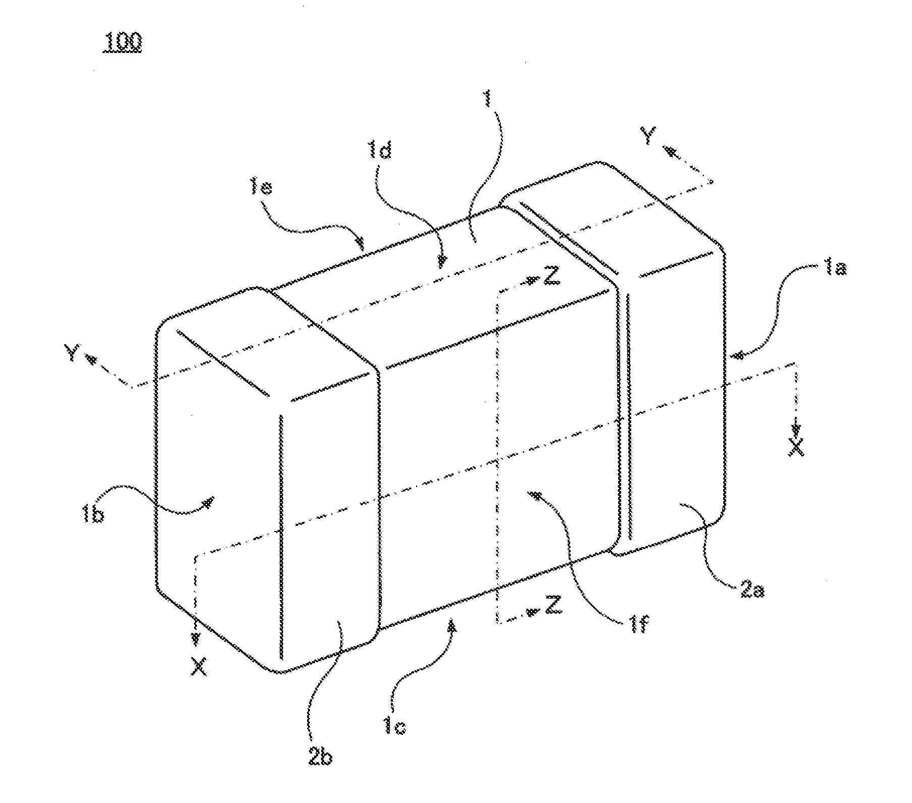
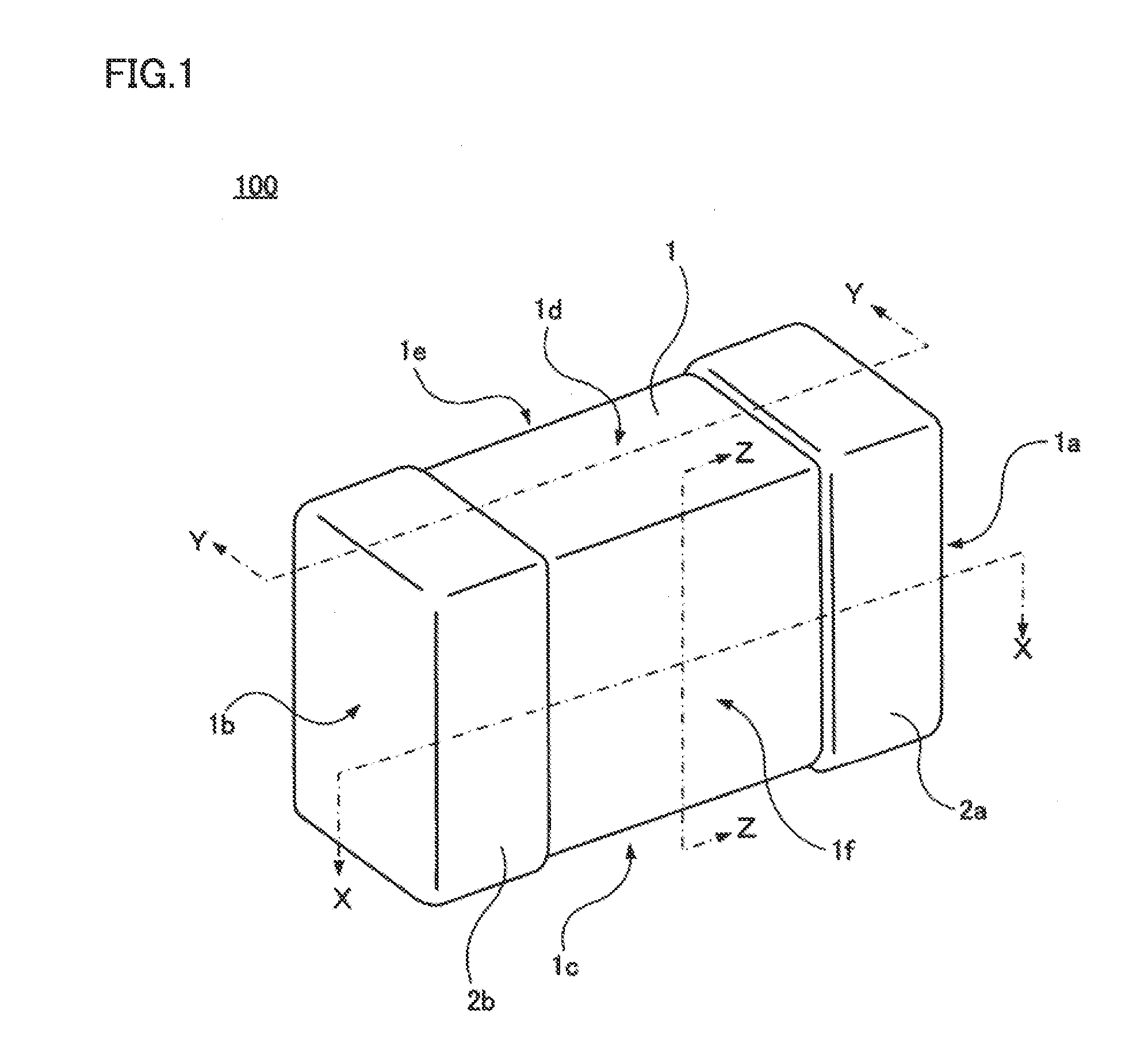
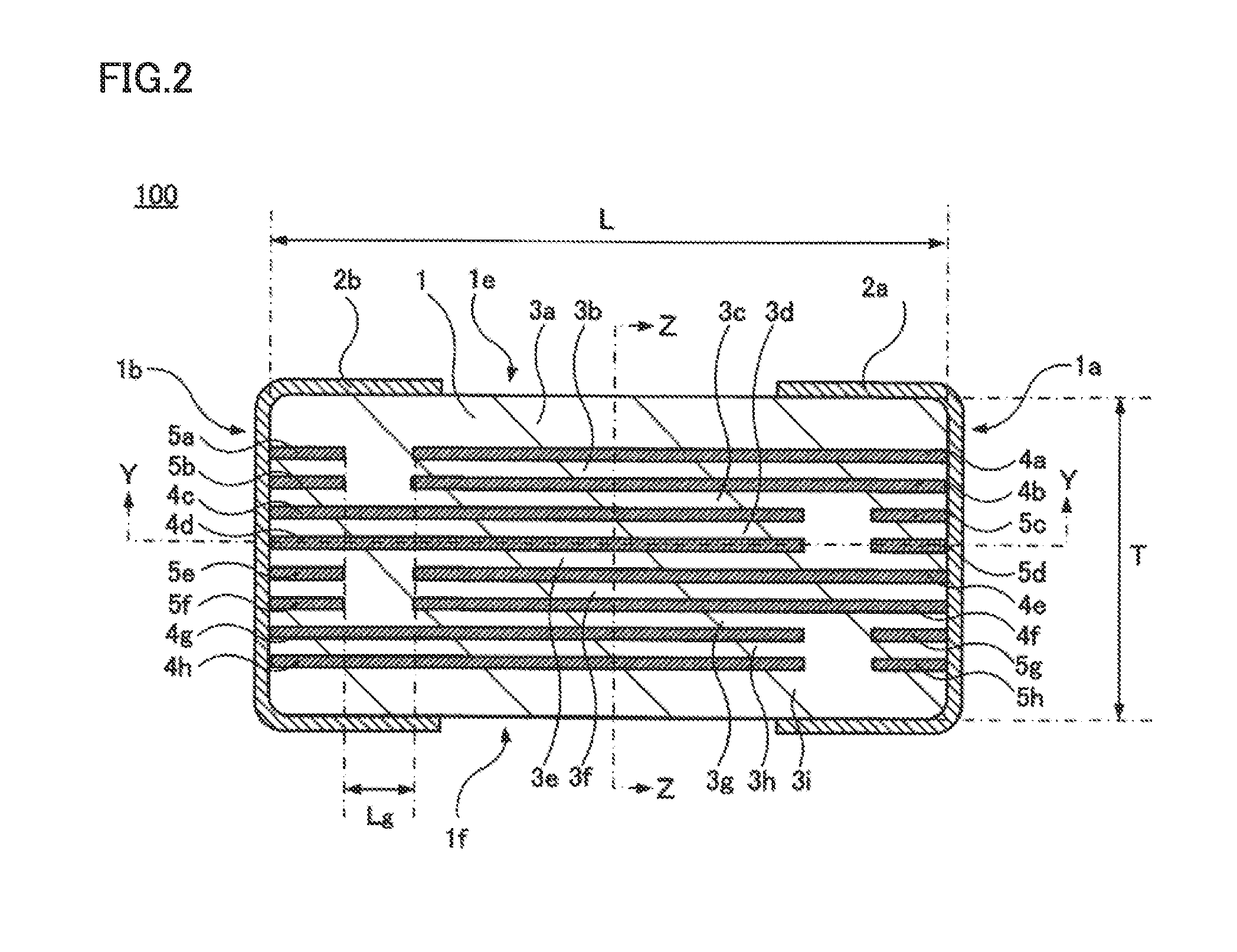
[0036]FIG. 1 is a perspective view showing a multilayer ceramic capacitor according to the first preferred embodiment of the present invention. FIG. 2 is a cross-sectional view of the multilayer ceramic capacitor according to the first preferred embodiment of the present invention, as seen in the direction indicated by line arrows X-X in FIG. 1. FIG. 3 is a cross-sectional view of the multilayer ceramic capacitor according to the first preferred embodiment of the present invention, as seen in the direction indicated by line arrows Y-Y in each of FIGS. 1 and 2. FIG. 4 is a cross-sectional view of the multilayer ceramic capacitor according to the first preferred embodiment of the present invention, as seen in the direction indicated by line arrows Z-Z in each of FIGS. 1 to 3.

[0037]As shown in FIGS. 1 to 4, a multilayer ceramic capacitor 100 includes a stacked body 1. The stacked body 1 preferably has a rectangular or substantially rectangular parallelepiped shape including a first end...

second preferred embodiment

[0098]A multilayer ceramic capacitor 200 according to the second preferred embodiment of the present invention will be hereinafter described. FIG. 10 is a cross-sectional view showing the configuration of a multilayer ceramic capacitor according to the second preferred embodiment of the present invention.

[0099]In the multilayer ceramic capacitor 100 according to the first preferred embodiment shown in each of FIGS. 1 to 4, two adjacent internal electrodes 4a and 4b are connected to one external electrode 2a, two adjacent internal electrodes 4c and 4d are connected to the other external electrode 2b, two adjacent internal electrodes 4e and 4f are connected to one external electrode 2a, and two adjacent internal electrodes 4g and 4h are connected to the other external electrode 2b. In this way, every two internal electrodes selected from internal electrodes 4a to 4h are defined as one set and connected to external electrode 2a or external electrode 2b. On the other hand, in multilayer...

experimental examples

[0107]The following experimental simulations were performed in order to confirm the effectiveness of the various preferred embodiments of the present invention.

[0108]First, as an Example, five types of multilayer ceramic capacitors each having the structure of the multilayer ceramic capacitor 100 according to the first preferred embodiment described above were formed. These five types of multilayer ceramic capacitors each had an electrostatic capacitance of about 0.7 pF, about 1.0 pF, about 1.5 pF, about 2.0 pF, and about 3.0 pF, respectively, for example.

[0109]In the Example, the stacked body 1 was configured to have a length dimension L of about 0.4 mm, a width dimension W of about 0.3 mm, and a thickness dimension T of about 0.2 mm.

[0110]Also, in the Example, the internal electrodes 14a to 14h each were configured to have a width dimension WE of about 0.2 mm that was about 68% of the width dimension W of stacked body 1. The thickness dimension TE of each of the internal electrode...


PUM

PropertyMeasurementUnit
Lengthaaaaaaaaaa
Lengthaaaaaaaaaa
Lengthaaaaaaaaaa

Abstract

A multilayer ceramic capacitor includes a stacked body including a stack of a plurality of dielectric layers and a plurality of internal electrodes, and a pair of external electrodes. In the stacked body, a width dimension is greater than a thickness dimension, a length dimension preferably is about 0.4 mm or less, a width dimension preferably is about 0.15 mm or more and about 0.35 mm or less, a thickness dimension preferably is about 0.2 mm or less, and each of the internal electrodes is made of Cu or Ag as a main component and has a width dimension that is about 60% or more of the width dimension of the stacked body.

Description

BACKGROUND OF THE INVENTION[0001]1. Field of the Invention[0002]The present invention relates to a multilayer ceramic capacitor, a mounting structure of the multilayer ceramic capacitor, and a taped electronic component array.[0003]2. Description of the Related Art[0004]As electronic devices have been reduced in size in recent years, size reduction of multilayer ceramic capacitors used in these electronic devices have also been demanded.[0005]Also, since the operation frequency has been rising in electronic devices such as a power amplifier (PA) module, the multilayer ceramic capacitor used therein is also required to exhibit few losses, a low ESR (Equivalent Series Resistance) and a high Q value in a high frequency region. The high frequency region corresponds to a range of 100 MHz or more and 100 GHz or less, for example.[0006]Japanese Patent Laying-Open No. 2000-306762 discloses a multilayer ceramic capacitor in which a high Q value is implemented in a high frequency region.[0007...

Claims


Application Information

Patent Timeline
IPC IPC(8): H05K1/18H01G4/248H01G4/232H01G4/012H05K1/02H01G4/30H01G4/12
CPCH05K1/181H01G4/30H01G4/248H05K2201/10015H01G4/012H05K1/0296H01G4/232H01G4/12H01G4/0085Y02P70/50
Inventor TERAOKA, EIJI
Owner MURATA MFG CO LTD
Why Eureka
Try Eureka