Stacked devices
- Summary
- Abstract
- Description
- Claims
- Application Information
AI Technical Summary
Benefits of technology
Problems solved by technology
Method used
Image


Examples
Embodiment Construction
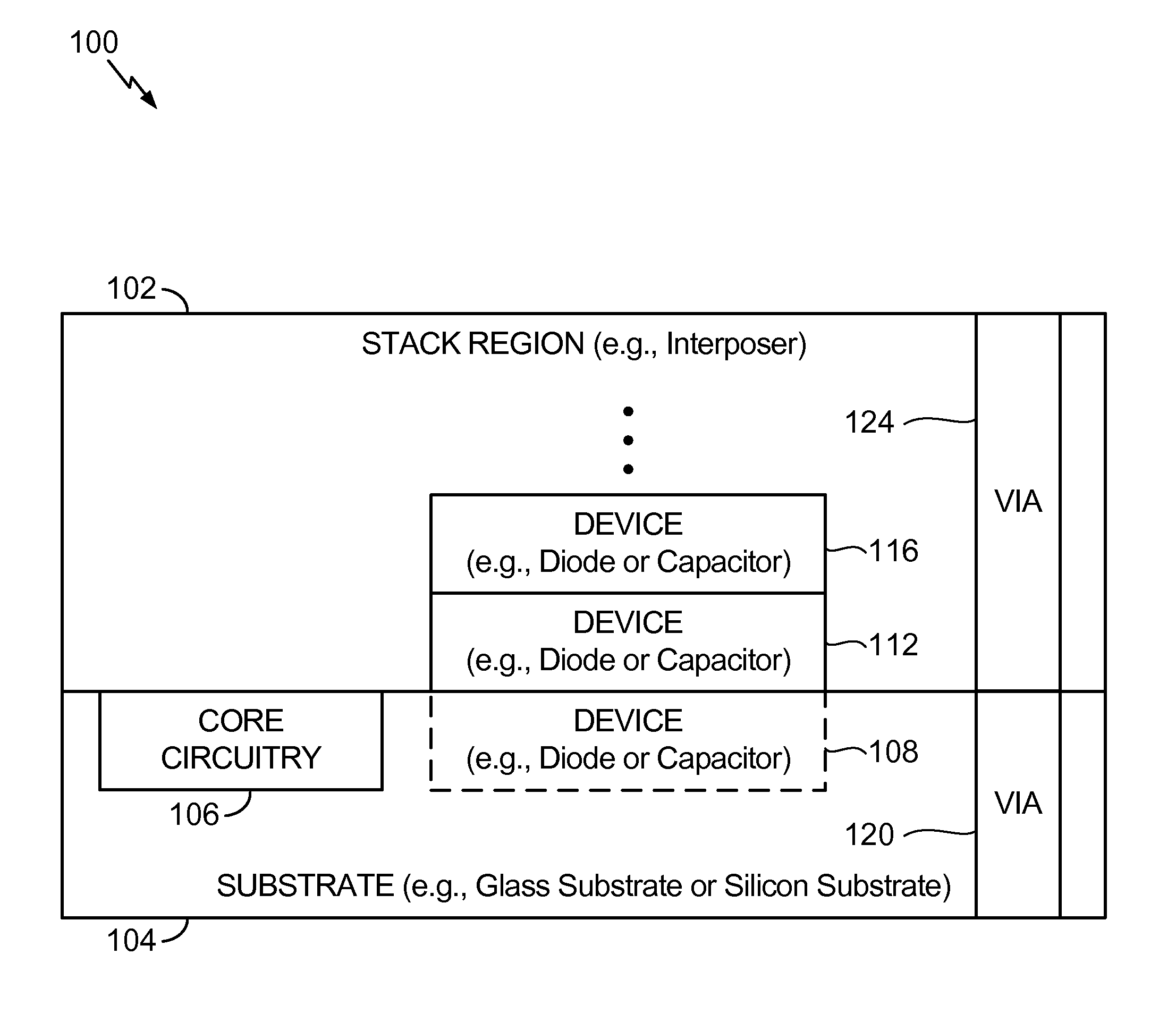
[0020]FIG. 1 illustrates an electronic device 100. The electronic device 100 includes a stack region 102 and a substrate 104. The substrate 104 may correspond to a silicon substrate or a glass substrate and may be included in a die (e.g., a semiconductor die cut from a semiconductor wafer). The stack region 102 may include a glass material, an isolation material, or a dielectric material, such as an oxide, a nitride, and / or a polymer, as illustrative examples. The substrate 104 may include core circuitry 106 and a via 120. The via 120 may be a through-substrate via (TSV) (or through-silicon via) that is disposed within (e.g., extends through) the substrate 104. The stack region 102 may include a via 124. The via 124 may extend through the stack region 102.
[0021]The stack region 102 and the substrate 104 include devices 108, 112, and 116 that are arranged in a stacked configuration. In FIG. 1, the device 108 is formed within the substrate 104, the device 112 is formed on (e.g., “stac...
PUM
 Abstract
Description
Claims
Application Information
 - R&D
- Intellectual Property
- Life Sciences
- Materials
- Tech Scout
- Unparalleled Data Quality
- Higher Quality Content
- 60% Fewer Hallucinations
Browse by: Latest US Patents, China's latest patents, Technical Efficacy Thesaurus, Application Domain, Technology Topic, Popular Technical Reports.
© 2025 PatSnap. All rights reserved.Legal|Privacy policy|Modern Slavery Act Transparency Statement|Sitemap|About US| Contact US: help@patsnap.com