Inductor, circuit board, and implementing method of the inductor

a technology of inductors and circuit boards, applied in the field of power electronic technology, can solve the problems of increasing the production cost of circuit boards, and achieve the effects of reducing the length of holes, reducing the production difficulty and cost of buried holes or blind holes, and reducing the cost of circuit boards

Active Publication Date: 2016-08-18
TCL CHINA STAR OPTOELECTRONICS TECH CO LTD
View PDF4 Cites 0 Cited by
  • Summary
  • Abstract
  • Description
  • Claims
  • Application Information

AI Technical Summary

Benefits of technology

[0017]The maximum inductance value of the hole in the circuit board, i.e., the inductance value of a through hole, is relatively fixed. Thus, for some circuits which require a small inductance value, the required inductance value can be obtained by reducing the length of the hole (i.e., adopting a buried hole or a blind hole). However, in the process of production of circuit boards, the production difficulty and cost of the buried hole or the blind hole are significantly higher than those of the through hole. Therefore, in order to solve this problem, the present disclosure further provides an inductor with a smaller inductance value, which is formed by a plurality of via holes that are in parallel connection. Thus the process difficulty and cost of the circuit board can be effectively reduced, which would be beneficial to the cost and quality control for the producer.

Problems solved by technology

However, the utilization of the magnetic beads, although removes the noise, results in an overlarge circuit board, thus increasing the production cost of the circuit board.

Method used


Image

  • Inductor, circuit board, and implementing method of the inductor
  • Inductor, circuit board, and implementing method of the inductor
  • Inductor, circuit board, and implementing method of the inductor

Examples


embodiment 1

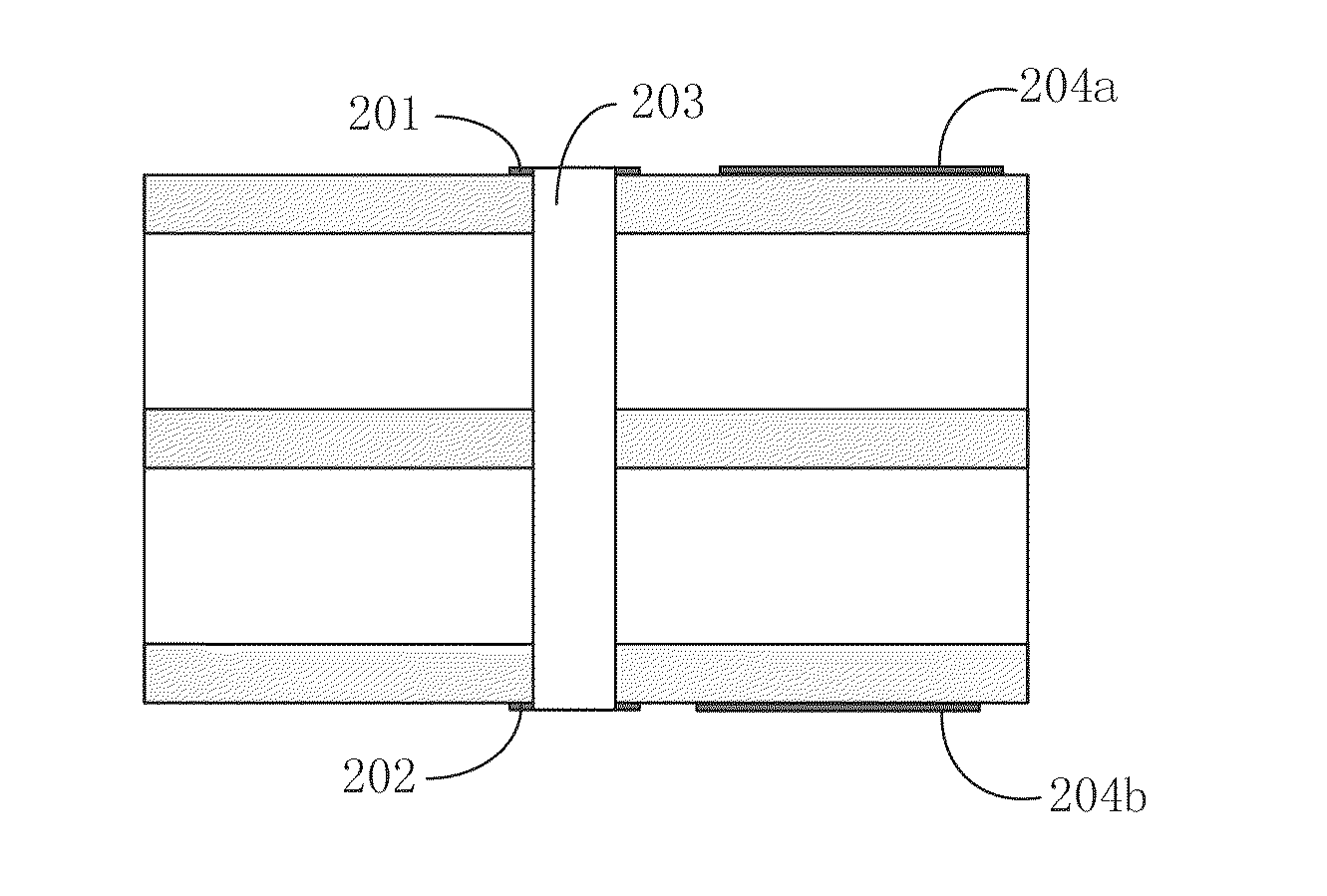
[0028]FIG. 2 schematically shows the structure of an inductor provided by embodiment 1.

[0029]As shown in FIG. 2, the inductor provided by the embodiment comprises a first pad 201, a second pad 202 and a first hole 203, wherein the first pad 201 is arranged on a first metal wiring layer 204a of a circuit board, and the second pad 202 is arranged on a second metal wiring layer 204b of the circuit board. One end of the first hole 203 is located in the first pad 201, while the other end thereof is located in the second pad 202. Meanwhile, conducting medium is filled in the first hole 203 to enable the first hole conductive.

[0030]Specifically, in the embodiment, a homogeneous and heat-shock-resistant layer of metallic copper is applied over the wall of the hole through metallization treatment. In particular, the metallization treatment comprises steps of desmear, chemical deposition with copper, copper intensification, and the like.

[0031]It is important to note that in other embodiments ...

embodiment 2

[0039]In circuit design, the thickness of the circuit board is constant. That is, the thickness of the circuit board is fixed after the number of layers and relevant parameters of the circuit board are determined. For a certain circuit board, since the thickness is fixed, the minimum diameter of the hole arranged on the circuit board is also relatively fixed. This is because the ratio of the diameter of the hole to the thickness of the circuit board cannot be less than a certain value due to processing requirement. Therefore, according to expression (1), the maximum inductance value of the hole is relatively fixed.

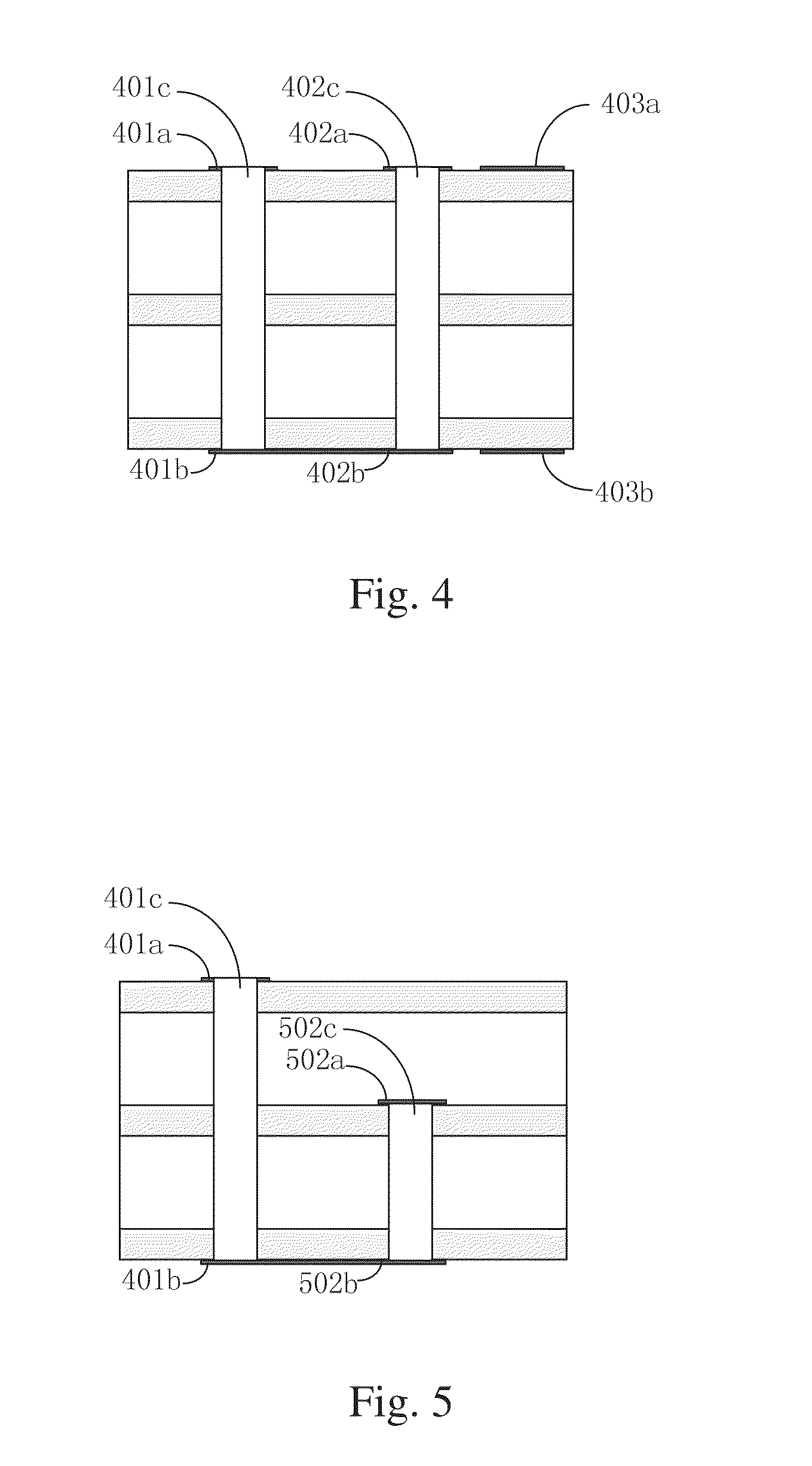
[0040]However, for different circuits, the inductance value required by the inductor in the circuits may exceed the maximum inductance value of the hole. Embodiment 2 provides a novel inductor in order to solve the problem. FIG. 4 schematically shows the structure of an inductor provided by the embodiment.

[0041]As shown in FIG. 4, the inductor provided by the embodiment co...

embodiment 3

[0047]It can be known from embodiment 2 that the maximum inductance value of the hole in the circuit board, i.e., the inductance value of a through hole, is relatively fixed. Thus, for some circuits which require a small inductance value, the required inductance value can be obtained by reducing the length of the hole (i.e., adopting a buried hole or a blind hole). However, in the production process of circuit boards, the production difficulty and cost of the buried hole or blind hole are significantly higher than those of the through hole. Therefore, in order to solve this problem, embodiment 3 of the present disclosure further provides an inductor as shown in FIG. 6.

[0048]As shown in FIG. 6, the inductor provided by the embodiment, similar to the inductor shown in FIG. 4, also comprises two pairs of pads and two holes, wherein a first pad 601a is connected with a third pad 602a through metal wirings, and a second pad 601b is also connected with a fourth pad 602b through metal wiri...


PUM


Abstract

An inductor, a circuit board and a method for forming an inductor are provided. The inductor comprises: a first pad arranged on a first metal wiring layer of a circuit board; a second pad arranged on a second metal wiring layer of the circuit board; and a first hole with conducting medium filled therein, one end of the first hole being located in the first pad and the other end thereof being located in the second pad. The inductor can effectively reduce the area of the circuit occupied by the inductor.

Description

CROSS REFERENCE TO RELATED APPLICATION[0001]The present application claims benefit of Chinese patent application CN 201410797963.9, entitled “Inductor, circuit board, and method for forming inductor” and filed on Dec. 18, 2014, which is incorporated herein by reference.TECHNICAL FIELD[0002]The present disclosure relates to the technical field of power electronic technology, and in particular, to an inductor, a circuit board, and a method for forming an inductor.TECHNICAL BACKGROUND[0003]In circuit board design, a magnetic bead is indicated by an inductor in terms of circuit symbol, i.e., the magnetic bead is the inductor. Magnetic bead has a small inductance value, is easy to manufacture, and possesses some other characteristics that cannot be achieved in many conventional inductors. For example, a conventional inductor may be equivalent to a capacitance under high frequency (especially high order harmonic) in view of distributed capacitance, so that it cannot function as an inducto...

Claims


Application Information

Patent Timeline
Patent Type & Authority Applications(United States)
IPC IPC(8): H05K1/16
CPCH05K1/165H05K3/46H05K2201/09627H05K2201/09672
Inventor FU, JIANYONG
Owner TCL CHINA STAR OPTOELECTRONICS TECH CO LTD
Why Eureka
Try Eureka