
Method For Manufacturing Assembly Of Flexible Display Device And Assembly Of Flexible Display Device Manufactured With Same

Active Publication Date: 2016-08-25
TCL CHINA STAR OPTOELECTRONICS TECH CO LTD
View PDF6 Cites 1 Cited by
  • Summary
  • Abstract
  • Description
  • Claims
  • Application Information

AI Technical Summary

Benefits of technology

The present invention provides a method for manufacturing an assembly of a flexible display device, which is simple and can protect the flexible base from heat. The method involves using a graphene layer to effectively conduct out heat generated during the manufacturing process, without increasing the thickness of a protective layer, reducing internal stress and facilitating thinning of the assembly. The resulting assembly has a simple structure, is less affected by heat and has improved quality.

Problems solved by technology

A flexible thin-film transistor (TFT) substrate is one of the key components of the flexible display device and selection and development of substrate material is the most important issue for the development of the flexible display device.
Laser activation generation a great amount of heat.
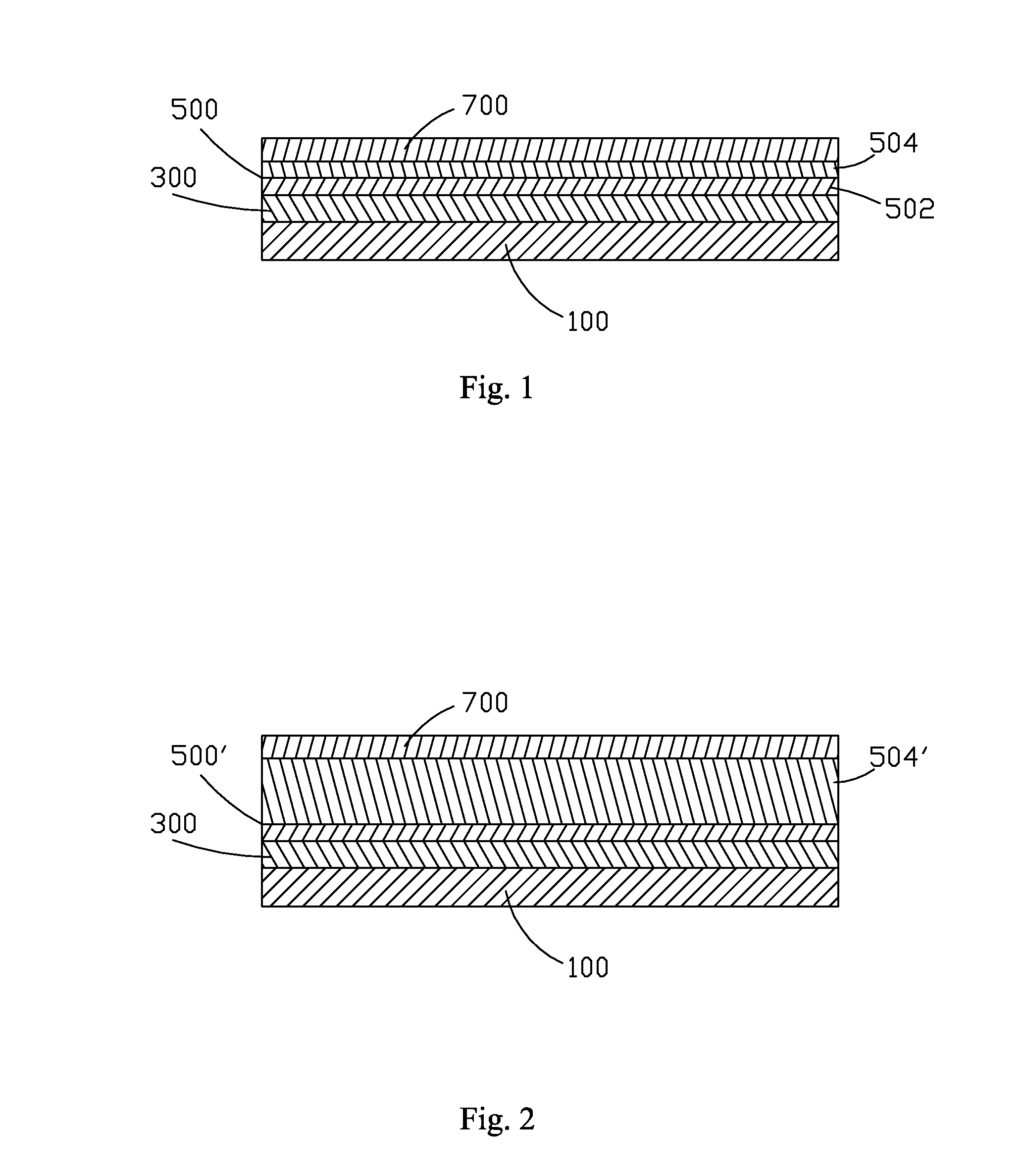
The heat, when transmitted to the flexible base 300, may cause deformation of the flexible base 300, severely affecting the quality of the flexible TFT substrate.
However, although such a measure reduces, to some extents, the possibility of deformation of the flexible base 300, an excessively large thickness of the silicon oxide layer 504′ would lead to an excessive stress, thereby affecting the curving performance of the flexible TFT substrate and also potentially causing other issues such as poor crystallization of the low-temperature polysilicon layer 700.

Method used


Image

  • Method For Manufacturing Assembly Of Flexible Display Device And Assembly Of Flexible Display Device Manufactured With Same
  • Method For Manufacturing Assembly Of Flexible Display Device And Assembly Of Flexible Display Device Manufactured With Same
  • Method For Manufacturing Assembly Of Flexible Display Device And Assembly Of Flexible Display Device Manufactured With Same

Examples


Embodiment Construction

[0040]To further expound the technical solution adopted in the present invention and the advantages thereof, a detailed description is given to a preferred embodiment of the present invention and the attached drawings.

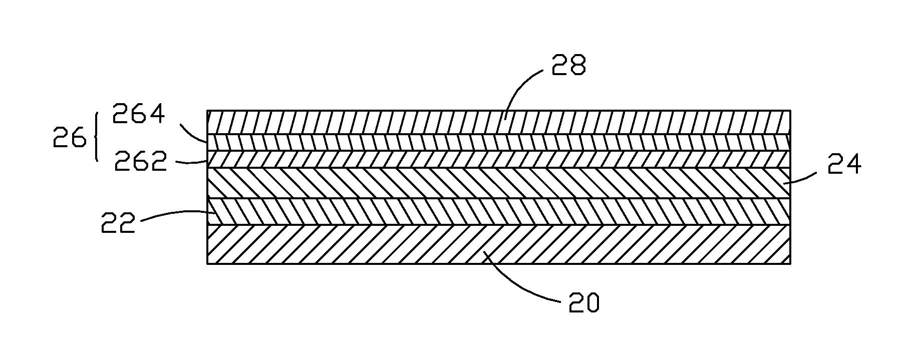
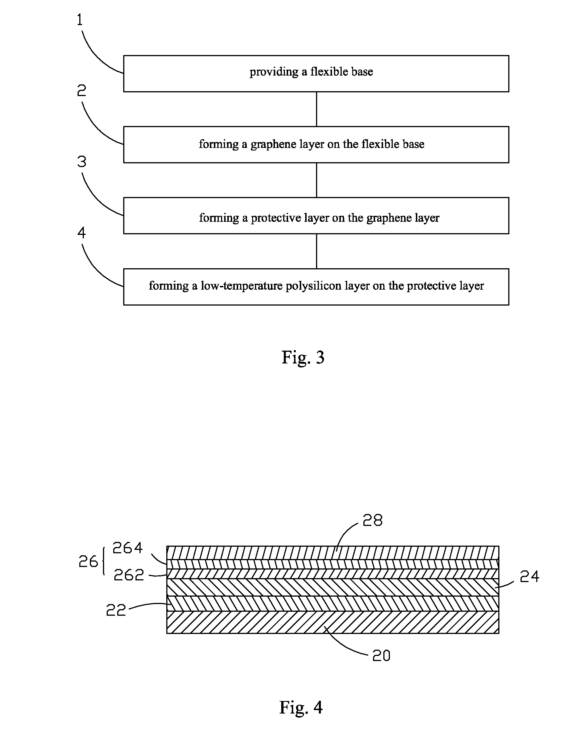
[0041]Referring to FIGS. 3 and 4, the present invention provides a method for manufacturing an assembly of a flexible display device, which comprises the following steps:

[0042]Step 1: providing a flexible base 22.

[0043]The flexible base 22 is made of polyethylene terephthalate (PET), polyethylene naphthalate (PEN), or polyimide (PI). In the instant embodiment, the flexible base 22 is formed on a glass substrate 20.

[0044]Step 2: forming a graphene layer 24 on the flexible base 22.

[0045]The graphene layer 24 is formed on the flexible base 22 by a process of microwave CVD (Chemical Vapor Deposition), transferring, or spin coating. Graphene is a material of a single-layered sheet structure formed of carbon atoms and a three-dimensional structure of grapheme has extremely h...


PUM


Abstract

The present invention provides a method for manufacturing an assembly of a flexible display device and an assembly of a flexible display device manufactured therewith. The method includes: (1) providing a flexible base (22); (2) forming a graphene layer (24) on the flexible base (22); (3) forming a protective layer (26) on the graphene layer (24); (4) forming a low-temperature polysilicon layer (28) on the protective layer (26). The method for manufacturing an assembly of a flexible display device and the assembly of the flexible display device manufactured therewith according to the present invention are such that the graphene layer is formed on the flexible base to effectively conduct out heat generated in the process of forming the low-temperature polysilicon layer so as to protect the flexible base from being affected by the heat without increasing the thickness of the protective layer thereby reducing internal stress and facilitating the realization of thinning.

Description

BACKGROUND OF THE INVENTION[0001]1. Field of the Invention[0002]The present invention relates to the field of displaying, and in particular to a method for manufacturing an assembly of a flexible display device and an assembly of a flexible display device manufactured with same.[0003]2. The Related Arts[0004]With the vivid and vigorous progress of displaying techniques and information devices, display devices have been evolved from the traditional cathode ray tubes (CRTs) to a flat panel display (FPD) era. A flexible display device, compared with a conventional rigid glass panel display device, possesses properties including being thinner and lighter, being flexible, being resistant to impact, and safety and is generally not constrained by location and space, thereby becoming the new trend of development of the next generation display devices.[0005]A flexible thin-film transistor (TFT) substrate is one of the key components of the flexible display device and selection and developmen...

Claims


Application Information

Patent Timeline
IPC IPC(8): H01L29/786H01L27/12
CPCH01L29/1606H01L29/78603H01L27/1218H01L29/78675H01L27/1262H01L27/1285H01L29/78606H01L27/1222H01L21/02422H01L21/02444H01L21/02488H01L21/02499H01L21/02502H01L21/02532
Inventor HU, GUOREN
Owner TCL CHINA STAR OPTOELECTRONICS TECH CO LTD
Learn More