Optical module including silicon photonics chip and coupler chip

a silicon photonics chip and optical module technology, applied in the field of optical modules, can solve the problems of not reaching the level of integration, cost and energy efficiency sufficient to supplant electrical interconnects on short links, electrical interconnects based on vertical cavity surface emitting lasers (vcsels) are, for example, ten times more expensive than electrical interconnects, and the cost associated with coupling light into and out of silicon photonic elements has limited commercial viability for optically based short links

Inactive Publication Date: 2016-09-15
SAMTEC
View PDF12 Cites 48 Cited by
  • Summary
  • Abstract
  • Description
  • Claims
  • Application Information

AI Technical Summary

Benefits of technology

[0041]The above and other features, elements, characteristics, steps, and advantages of the present invention will become more apparent from the following detailed description of preferred embodiments of the present invention with reference to the attached drawings.

Problems solved by technology

Although optical interconnects are already present in the heart of telecommunication networks (transoceanic networks, metropolitan and access networks, etc.), they have not yet reached the level of integration and cost and energy efficiency sufficient to supplant electrical interconnects on short links.
Optical interconnects based on vertical cavity surface emitting lasers (VCSELs) are, for example, still ten times more expensive than electrical interconnects.
The expense associated with coupling light into and out of a Silicon Photonics element has limited commercial viability for optically based short links.

Method used


Image

  • Optical module including silicon photonics chip and coupler chip
  • Optical module including silicon photonics chip and coupler chip
  • Optical module including silicon photonics chip and coupler chip

Examples


Embodiment Construction

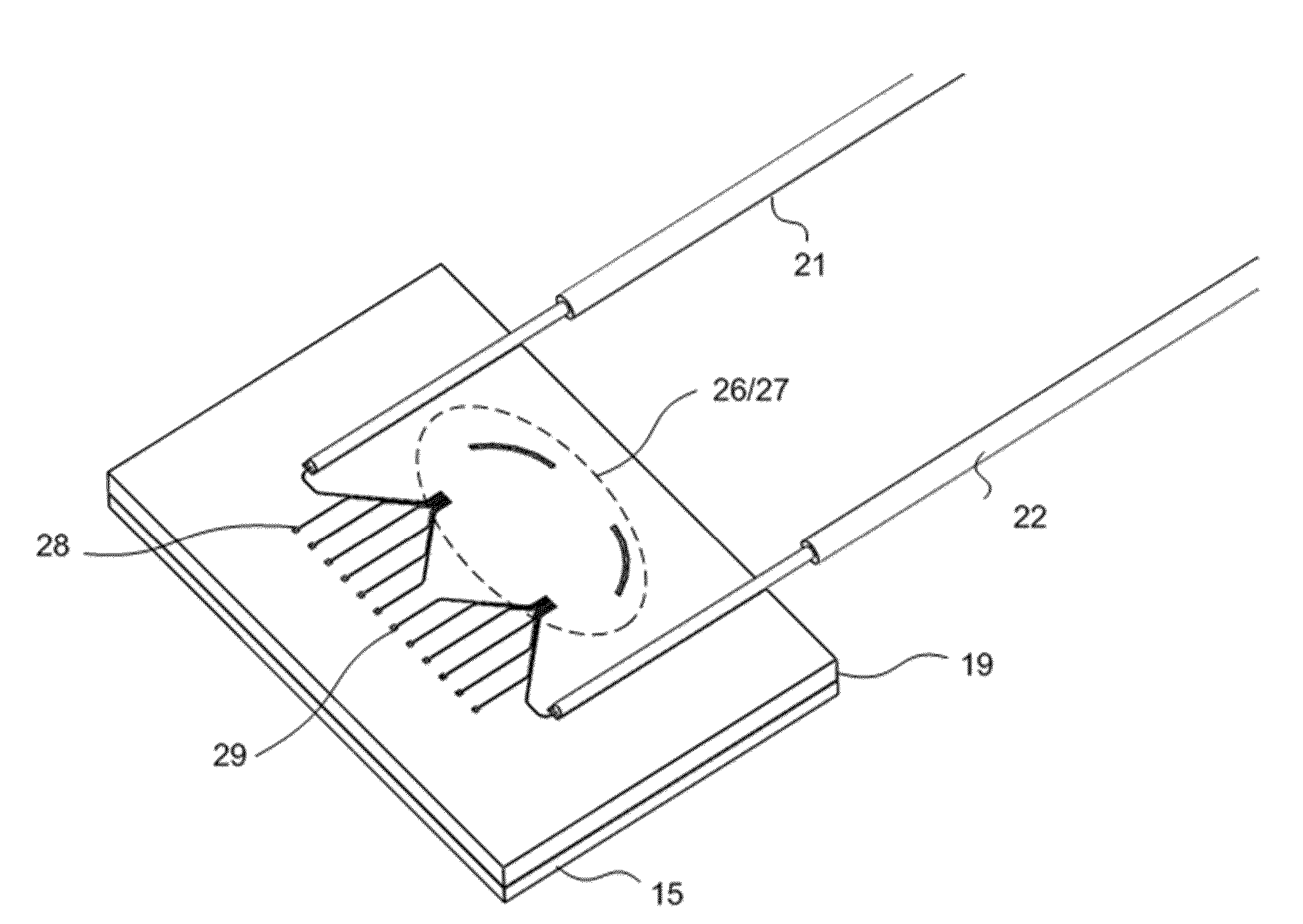
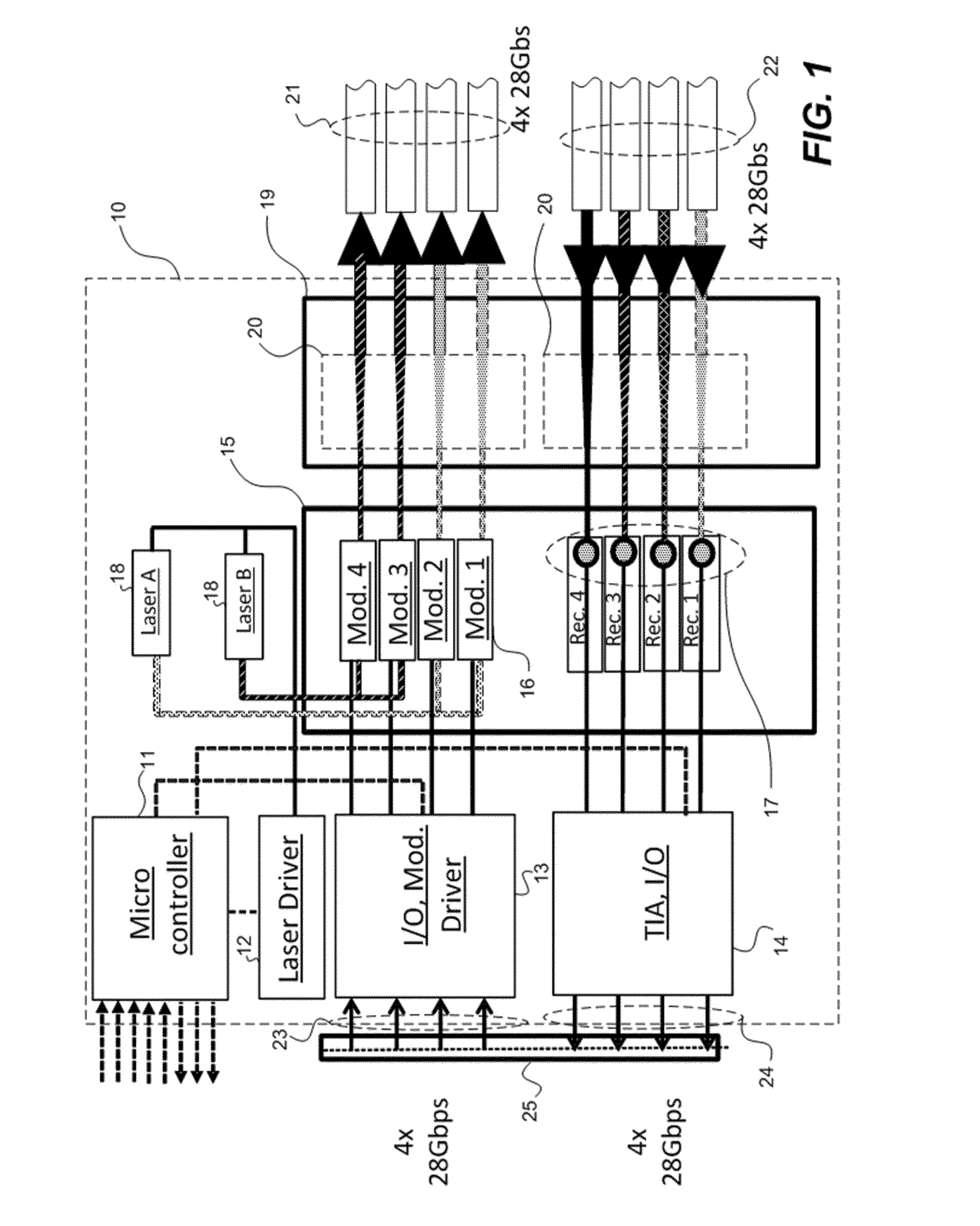
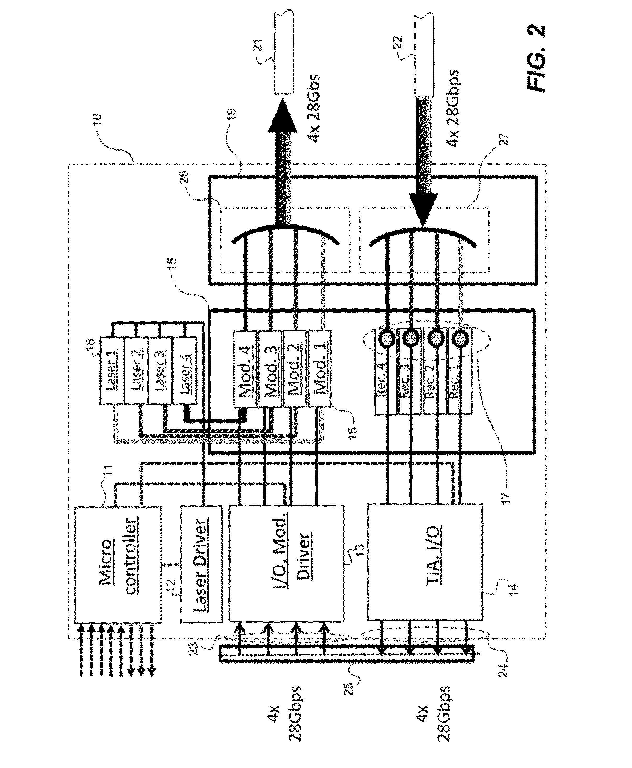
[0063]FIG. 1 shows a Silicon Photonics (SiPho) system according to a preferred embodiment of the present invention. Transceiver 10 includes a microcontroller 11 that is connected to laser driver 12, modulator driver 13, and transimpedance amplifier (TIA) 14. The microcontroller 11 receives and sends electrical auxiliary signals, including, for example, control and monitoring signals, from and to one or more devices external to the SiPho system as shown by the arrows on the right-hand side of microcontroller 10. The modulator driver 13 receives electrical data signals through transmission (Tx) inputs 23, and the TIA 14 outputs electrical data signals through reception (Rx) outputs 24. The Tx inputs 23 and the Rx outputs 24 are preferably included in connector 25. The lasers A, B (labeled as reference number 18) are connected to a laser driver 12. The transceiver 10 also includes a Silicon Photonics (SiPho) chip 15 and a coupler chip 19. The coupler chip 19 is connected to Tx waveguid...


PUM


Abstract

An optical module includes a waveguide interconnect that transports light signals; a Silicon Photonics chip that modulates the light signals, detects the light signals, or both modulates and detects the light signals; a coupler chip attached to the Silicon Photonics chip and the waveguide interconnect so that the light signals are transported along a light path between the Silicon Photonics chip and the waveguide interconnect; and one of the Silicon Photonics chip and the coupler chip includes first, second, and third alignment protrusions. The other of the coupler chip and the Silicon Photonics chip includes a point contact, a linear contact, and a planar contact. The point contact provides no movement for the first alignment protrusion. The linear contact provides linear movement for the second alignment protrusion. The planar contact provides planar movement for the third alignment protrusion.

Description

RELATED APPLICATIONS[0001]This application claims the benefit under 35 U.S.C. §119(e) to U.S. Application No. 62 / 131,971 filed on Mar. 12, 2015; U.S. Application No. 62 / 131,989 filed on Mar. 12, 2015; U.S. Application No. 62 / 132,739 filed on Mar. 13, 2015; U.S. Application No. 62 / 134,166 filed on Mar. 17, 2015; U.S. Application No. 62 / 134,173 filed on Mar. 17, 2015; U.S. Application No. 62 / 134,229 filed on Mar. 17, 2015; U.S. Application No. 62 / 158,029 filed on May 7, 2015; and U.S. Application No. 62 / 215,932 filed on Sep. 9, 2015. The entire contents of each of U.S. Application No. 62 / 131,971; 62 / 131,989; 62 / 132,739; 62 / 134,166; 62 / 134,173; 62 / 134,229; 62 / 158,029; and 62 / 215,932 are hereby incorporated herein by reference.BACKGROUND OF THE INVENTION[0002]1. Field of the Invention[0003]The present invention relates to optical modules. More specifically, the present invention relates to optical modules with Silicon Photonic devices.[0004]2. Description of the Related Art[0005]The use...

Claims


Application Information

Patent Timeline
Patent Type & Authority Applications(United States)
IPC IPC(8): G02B6/30G02B6/42G02B6/12
CPCG02B6/305G02B6/12004G02B6/423G02B2006/12164G02B2006/12142G02B2006/12123G02B2006/12102G02B6/4292G02B6/12007G02B6/1228G02B6/124G02B6/138G02B6/2938G02B6/3652G02B6/4214G02B6/428
Inventor EPITAUX, MARCCORNELIUS, JOSHUA RAJIVNIGHTINGALE, JOHN L.
Owner SAMTEC
Why Eureka
Try Eureka