Semiconductor devices including shallow trench isolation (STI) liners

a technology of shallow trench isolation and semiconductor devices, which is applied in the direction of semiconductor devices, electrical equipment, transistors, etc., can solve problems such as defects, and achieve the effect of reducing or possibly preventing an occurrence of transistor defects

Inactive Publication Date: 2016-09-22
SAMSUNG ELECTRONICS CO LTD
View PDF5 Cites 23 Cited by
  • Summary
  • Abstract
  • Description
  • Claims
  • Application Information

AI Technical Summary

Benefits of technology

[0008]Aspects of the present inventive concept provide a semiconductor device which is capable of reducing or possibly preventing an occurrence of defect in the transistor,

Problems solved by technology

However, there has been a problem that, in the process of removing the native oxide before growth of an epitaxial layer, a part of a device isolation

Method used


Image

  • Semiconductor devices including shallow trench isolation (STI) liners
  • Semiconductor devices including shallow trench isolation (STI) liners
  • Semiconductor devices including shallow trench isolation (STI) liners

Examples


first embodiment

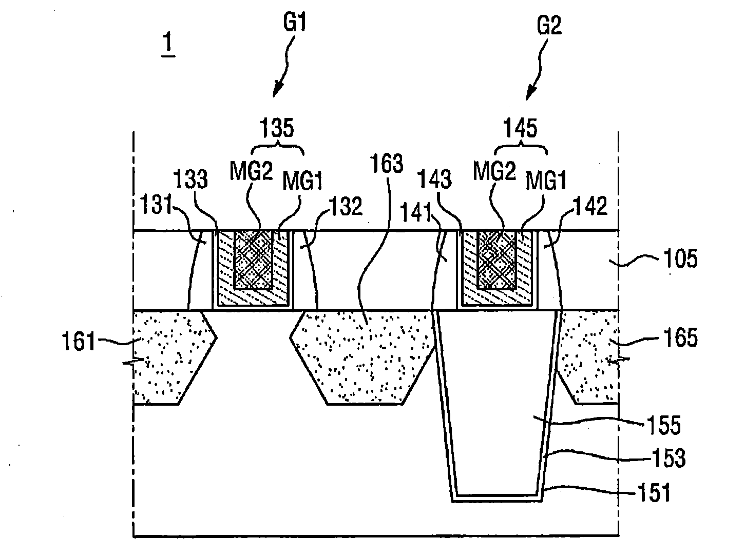
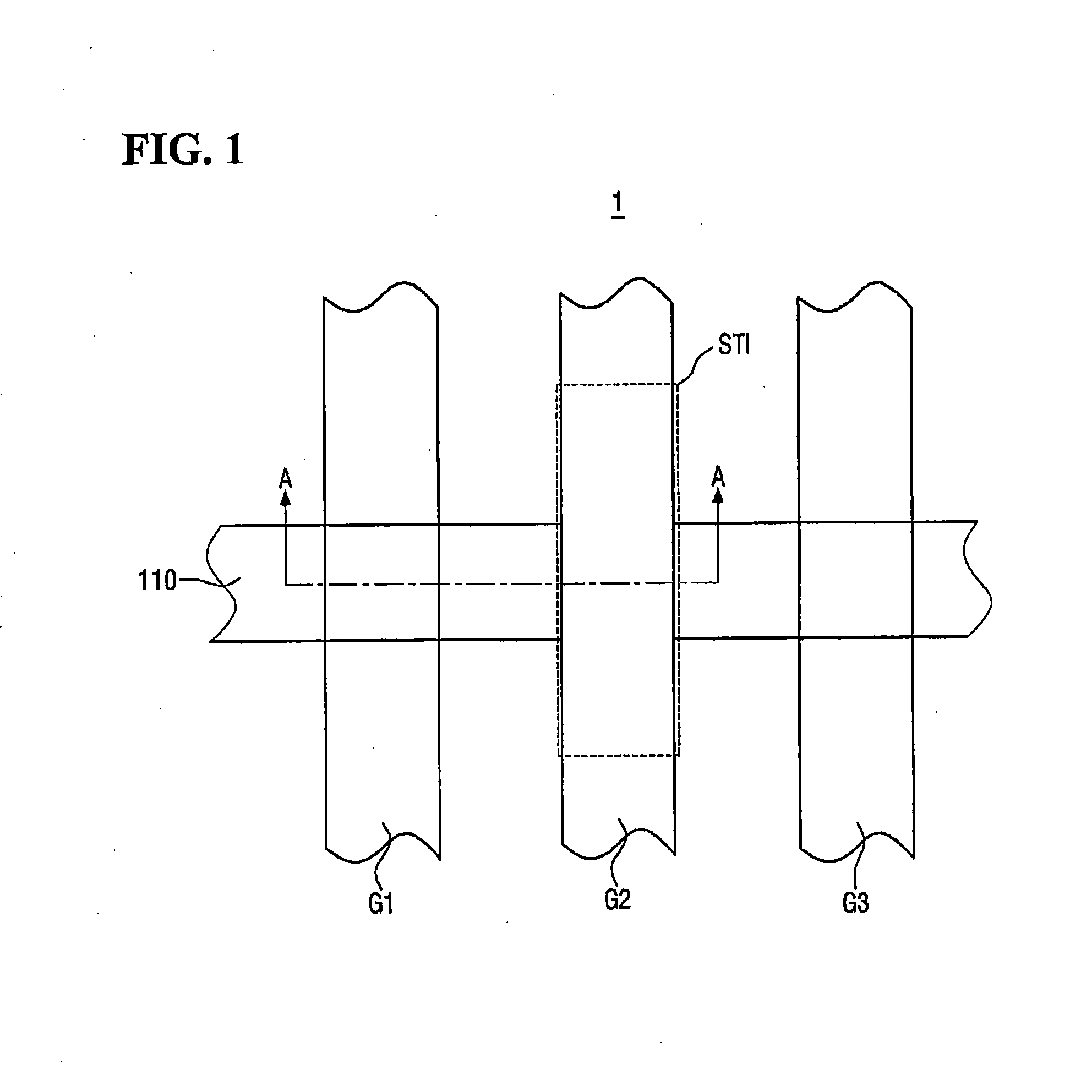
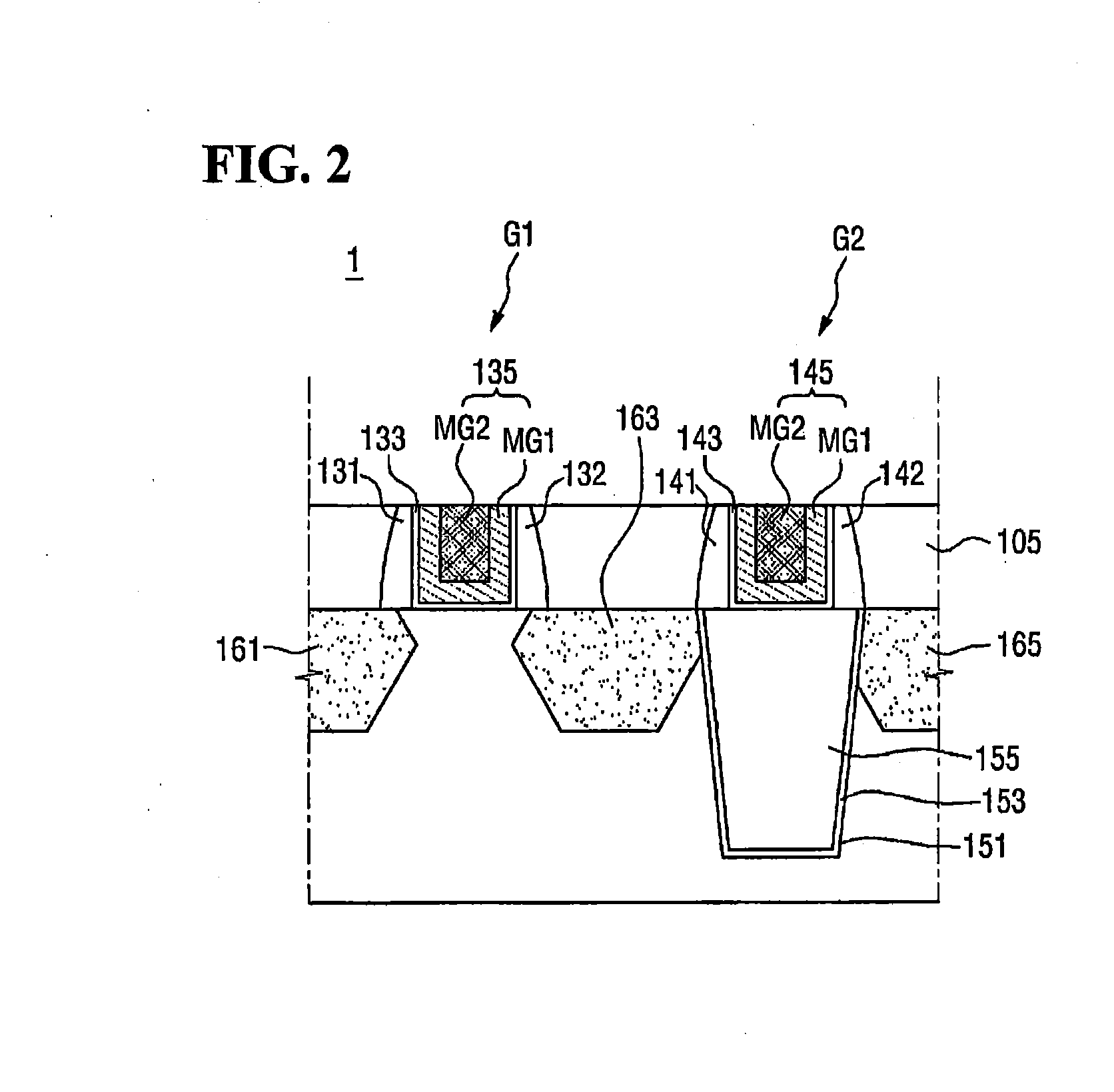
[0045]FIG. 1 is a diagram for explaining a semiconductor device according to the present inventive concept. FIGS. 2 and 3 are cross-sectional views taken along a line A-A of FIG. 1.

[0046]Referring to FIG. 1, a semiconductor device 1 includes a substrate 100, an active region 110, a first gate structure G1, a second gate structure G2 and a device isolation film (STI) 155.

[0047]The substrate 100, for example, may be a semiconductor substrate. The substrate 100 may include one of silicon, strained silicon, silicon alloy, silicon carbide (SiC), silicon germanium (SiGe), silicon germanium carbide (SiGeC), germanium, germanium alloy, gallium arsenide (GaAs), indium arsenide (InAs), an III-V semiconductor, and an II-VI semiconductor, combinations thereof, and laminations thereof. Also, if necessary, the substrate may be an organic plastic substrate rather than the semiconductor substrate. Hereinafter, the substrate 100 will be described as being made up of silicon.

[0048]The substrate 100 m...

second embodiment

[0072]FIG. 4 is a diagram for explaining a semiconductor device according to the present inventive concept. FIG. 5 is a cross-sectional view taken along a line B-B of FIG. 4. For convenience of explanation, hereinafter, the repeated description of the same matters as the previous embodiment will not be provided, and the description will be provided while focusing on the differences.

[0073]Referring to FIGS. 4 and 5, a semiconductor device 2 according to a second embodiment of the present inventive concept may be formed in the substantially similar manner to the semiconductor device 1 according to the above-mentioned first embodiment of the present inventive concept. The first gate structure G4 may be disposed on the active region 110, and the second gate structure G5 may be disposed on a device isolation film 255.

[0074]However, the second gate structure G5 of the semiconductor device 2 according to the second embodiment may be disposed so as to be in contact with only the upper surfa...

third embodiment

[0076]FIG. 6 is a diagram for explaining a semiconductor device according to the present inventive concept. FIG. 7 is a cross-sectional view taken along a line C-C of FIG. 6. For convenience of explanation, hereinafter, the repeated description of the same matters as the previous embodiment will not be provided, and the description will be provided while focusing on the differences.

[0077]Referring to FIGS. 6 and 7, a semiconductor device 3 according to the third embodiment of the present inventive concept may be formed in the substantially similar manner to the above-mentioned semiconductor device 1 according to the second embodiment of the present inventive concept. However, the semiconductor device 3 according to the third embodiment may further include a third gate structure G9.

[0078]At this time, the first gate structure G7 may be disposed on the active region 110, and the second gate structure G8 and the third gate structure G9 may be disposed on a device isolation film 355. Th...


PUM


Abstract

Semiconductor devices including STI liners are provided. The semiconductor devices may include a STI trench that defines an active region in a substrate, a STI liner that extends conformally along side walls and a bottom surface of the STI trench, a device isolation film that is on the STI liner and fills up at least a part of the STI trench, a first gate structure that is disposed on the active region, and a second gate structure that is spaced apart from the first gate structure. The second gate structure may include a gate insulating film contacting the device isolation film, a gate electrode on the gate insulating film, and spacers on both sides of the gate electrode. Lower surfaces of the spacers may contact an upper surface of the STI liner.

Description

CROSS-REFERENCE TO RELATED APPLICATION[0001]This U.S. non-provisional patent application claims priority under 35 U.S.C. §119 to Korean Patent Application No. 10-2015-0037177 filed on Mar. 18, 2015 in the Korean intellectual Property Office, the disclosure of which is hereby incorporated by reference in its entirety.BACKGROUND[0002]1. Technical Field[0003]The present inventive concept relates to a semiconductor device having a STI liner.[0004]2. Discussion of Related Art[0005]Recently, semiconductor devices have been developed to provide a high-speed operation at a low voltage, and manufacturing processes of a semiconductor device have been developed to increase integration degree.[0006]The increased integration degree of the device may cause a short channel effect or the like on a field effect transistor (FET) as one of a semiconductor device. Therefore, in order to overcome this problem, researches of a fin field effect transistor (Fin FET) in which channels are formed by a three-...

Claims


Application Information

Patent Timeline
IPC IPC(8): H01L27/088H01L29/423H01L27/12H01L29/78H01L29/06
CPCH01L27/0886H01L29/785H01L29/42356H01L27/1211H01L29/0653H01L21/823431H01L21/823468H01L21/823481H01L27/088H01L21/823821H01L27/0924H01L21/76283H01L21/76831H01L29/7846
Inventor LIM, SUN-MELIM, YOUNG-DALCHO, HAG-JU
Owner SAMSUNG ELECTRONICS CO LTD
Why Eureka
Try Eureka