Method for atomic layer etching

a layer etching and layer technology, applied in the direction of electrical equipment, electrical discharge tubes, chemistry apparatus and processes, etc., can solve the problems of imposing ever-increasing challenges on the ability, and achieve the effect of facilitating the etching process and facilitating the etching process

Active Publication Date: 2016-10-06
TOKYO ELECTRON LTD
View PDF5 Cites 28 Cited by
  • Summary
  • Abstract
  • Description
  • Claims
  • Application Information

AI Technical Summary

Benefits of technology

[0008]Embodiments of the invention relate to a method for patterning a layer, and more specifically, to a method for etching a layer.
[0009]According to one embodiment, a method of etching a layer on a substrate is described. A method of etching a layer on a substrate includes disposing the substrate in a plasma processing system configured to facilitate an etching process, performing an atomic layer etching process cycle to etch a monolayer of an exposed surface of the substrate, and repeating the atomic layer etching process cycle until a target depth is reached. Each process cycle etches the monolayer from the exposed surface. The atomic layer etching process cycle sequentially includes forming an adsorption monolayer comprising an etchant on an exposed surface of the substrate by introducing the etchant while concurrently coupling electromagnetic power to the plasma processing system at a power level targeted to achieve an etchant radical flux at the substrate greater than a total ion flux at the substrate, which power level is less than or equal to 50 W, purging ...

Problems solved by technology

These trends and requirements impose ever-increasing challenges on t...

Method used


Image

  • Method for atomic layer etching
  • Method for atomic layer etching
  • Method for atomic layer etching

Examples


Embodiment Construction

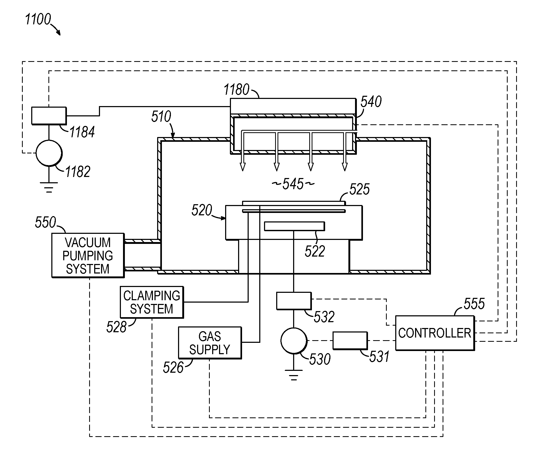
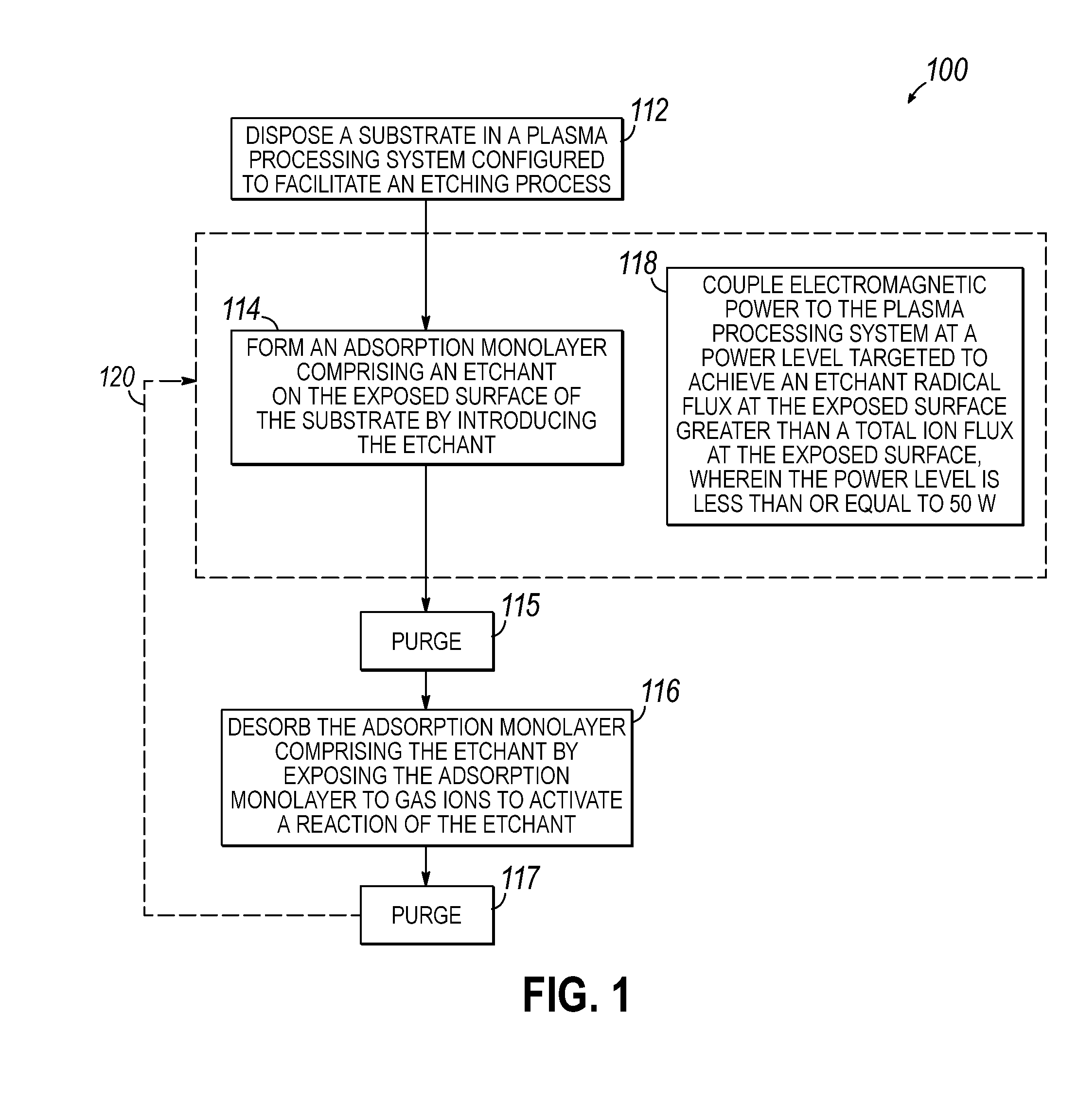
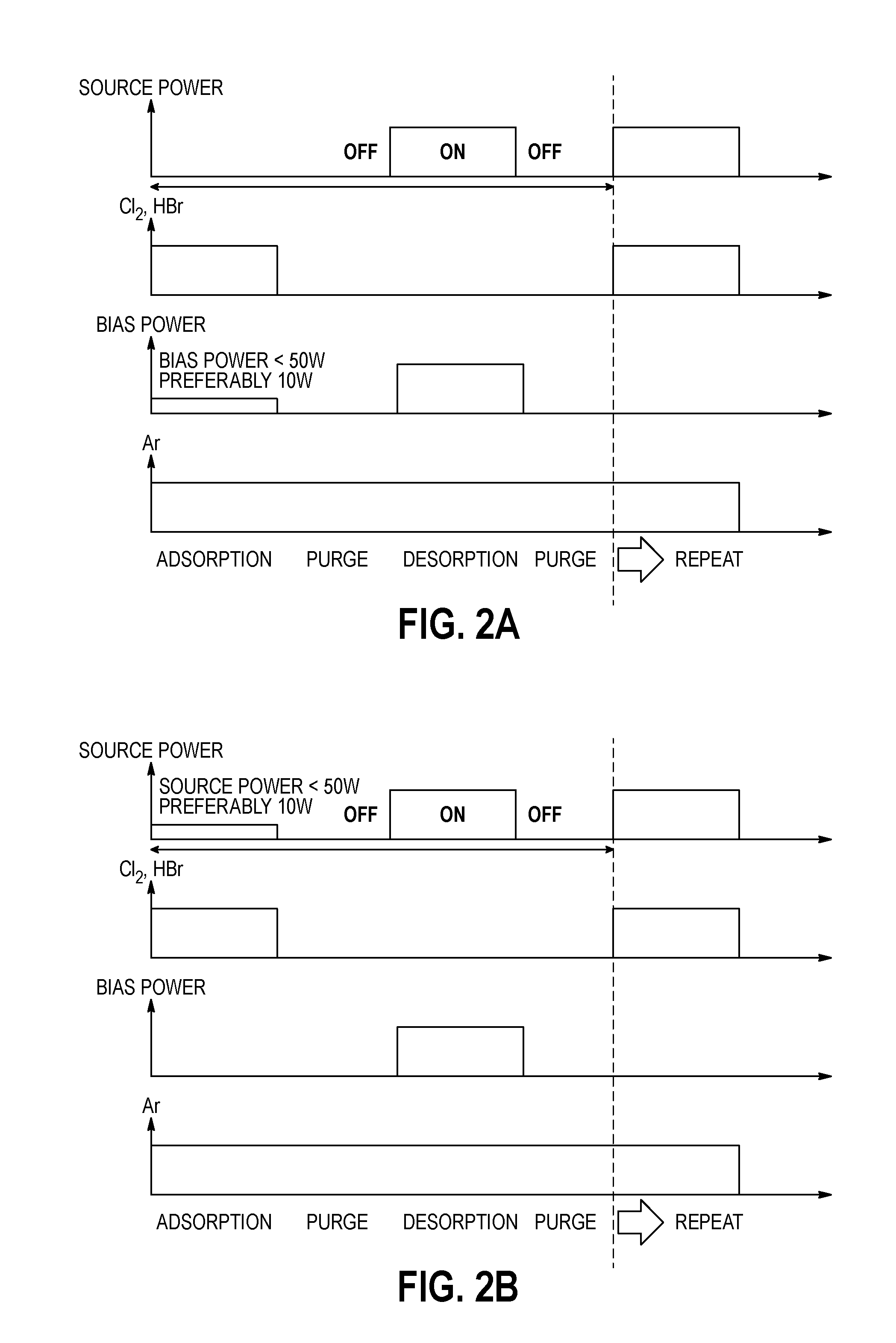
[0023]In the following description, for purposes of explanation and not limitation, specific details are set forth, such as a particular geometry of a processing system, descriptions of various components and processes used therein. However, it should be understood that the invention may be practiced in other embodiments that depart from these specific details.

[0024]Similarly, for purposes of explanation, specific numbers, materials, and configurations are set forth in order to provide a thorough understanding of the invention. Nevertheless, the invention may be practiced without specific details. Furthermore, it is understood that the various embodiments shown in the figures are illustrative representations and are not necessarily drawn to scale.

[0025]Various operations will be described as multiple discrete operations in turn, in a manner that is most helpful in understanding the invention. However, the order of description should not be construed as to imply that these operations...


PUM


Abstract

A method of etching a layer on a substrate includes disposing a substrate in a plasma processing system configured to facilitate an etching process, performing an atomic layer etching process cycle to etch a monolayer of an exposed surface of the substrate, and repeating the atomic layer etching process cycle until a target depth is reached. Each process cycle etches the monolayer from the exposed surface. The atomic layer etching process cycle sequentially includes forming an adsorption monolayer comprising an etchant on an exposed surface of the substrate by introducing the etchant while concurrently coupling electromagnetic power to the plasma processing system at a power level targeted to achieve an etchant radical flux at the substrate greater than a total ion flux at the substrate, which power level is less than or equal to 50 W, purging the plasma processing system to remove any excess etchant, desorbing the adsorption monolayer by exposing the adsorption monolayer to gas ions to activate a reaction of the etchant, and purging the plasma processing system again.

Description

CROSS-REFERENCE TO RELATED APPLICATIONS[0001]This application is related and claims priority to U.S. Provisional Patent Application Ser. No. 62 / 139,795 filed on Mar. 30, 2015, the entire contents of which are herein incorporated by reference.FIELD OF INVENTION[0002]The invention relates to a method for patterning a layer, and more specifically, to a method for etching a layer.DESCRIPTION OF RELATED ART[0003]The need to remain competitive in cost and performance in the production of semiconductor devices elevates demand to continually increase the device density of integrated circuits. And, to achieve higher degrees of integration with the miniaturization in semiconductor integrated circuitry, robust methodologies are required to reduce the scale of the circuit pattern formed on the semiconductor substrate. These trends and requirements impose ever-increasing challenges on the ability to transfer the circuit pattern from one layer to another layer.[0004]Photolithography is a mainstay...

Claims


Application Information

Patent Timeline
IPC IPC(8): H01L21/3065
CPCH01L21/3065H01J37/32963C09K13/00H01L21/31116H01L21/32136
Inventor RANJAN, ALOKSHERPA, SONAMWANG, MINGMEI
Owner TOKYO ELECTRON LTD
Why Eureka
Try Eureka