Quantum information processing

a technology of information processing and quantum dots, applied in the field of quantum information processing, can solve the problems of limiting the initialisation, manipulation and reading of qubits, and current quantum dot-based systems that are not practical, and achieve the effects of reducing and limiting the number of qubits

a technology of information processing and quantum dots, applied in the field of quantum information processing, can solve the problems of limiting the initialisation, manipulation and reading of qubits, and current quantum dot-based systems that are not practical, and achieve the effects of reducing and limiting the number of qubits

US20160300155A1Active Publication Date: 2016-10-13HITACHI LTD

Image

  • Quantum information processing
  • Quantum information processing
  • Quantum information processing

Examples


Embodiment Construction

[0072]1 Well-Defined Qubits

[0073]1.1 Architecture

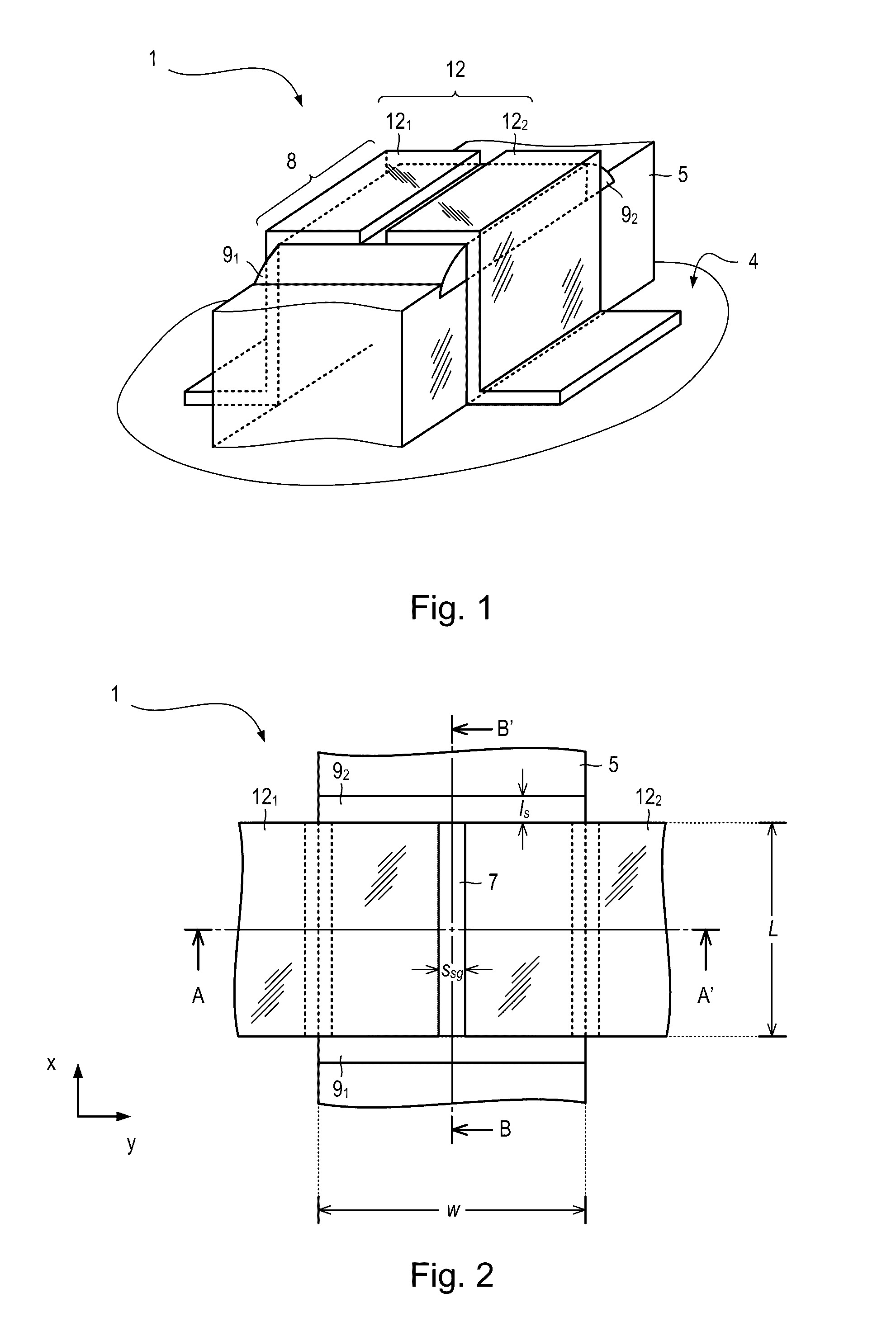
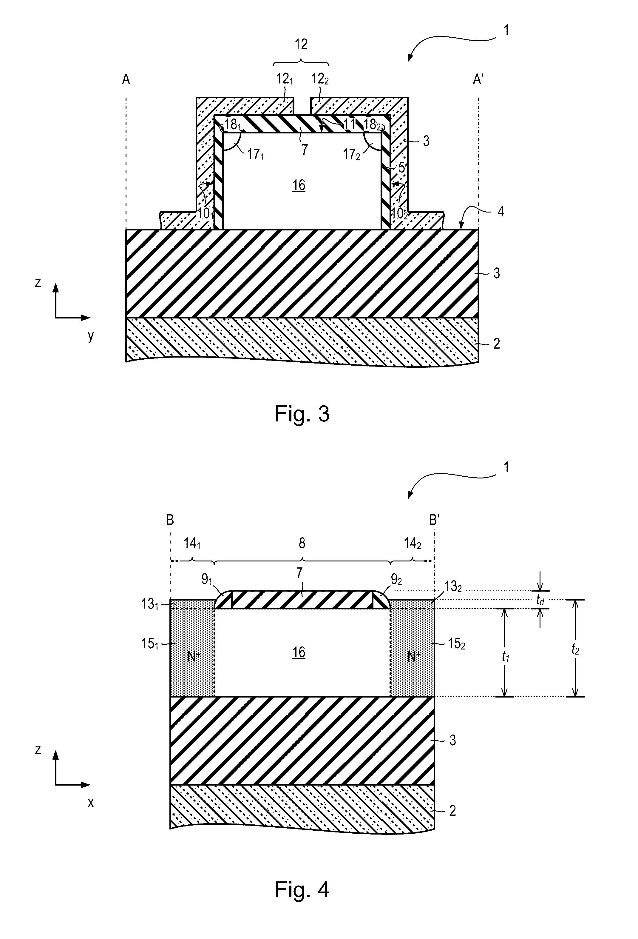
[0074]Referring to FIG. 1 to FIG. 4, a silicon nanowire field-effect transistor 1 is shown.

[0075]The transistor 1 comprises a silicon substrate 2 and a silicon dioxide layer 3 having an upper surface 4 disposed on the substrate 2. An elongate conductive mesa 5 (or “channel”) which is generally rectangular in cross section is disposed on the upper surface 4 of the dielectric layer 3 and runs in a first direction (along the x-axis). A gate dielectric 7 (best shown in FIG. 3) is disposed on a first section 8 of the mesa 4 between first and second silicon nitride spacer elements 91, 92 (which may also be referred to simply as “spacers”). The gate dielectric 7 comprises hafnium silicon oxynitride (HfSiON) or other high-k dielectric with an equivalent oxide thickness of less than 2 nm so as to provide strong gate-channel coupling. The gate dielectric 7 is formed on first and second faces 101, 102 and a top face 11 of the mesa 5. A split-gat...


PUM


Abstract

Quantum information processing apparatus and methods are described. The apparatus comprises a device for defining a qubit and a reflectometry circuit for reading out a state of the qubit. The device comprises a semiconductor nanowire extending along a first direction having first and second obtuse or acute edges running along the first direction, gate dielectric overlying the first and second edges of the nanowire and a split gate running across a section of the nanowire in a second, transverse direction, the split gate comprising first and second gates overlying the first and second edges respectively. The reflectometry circuit comprises a resonator coupled to the first or second gate.

Description

CROSS REFERENCE TO PRIOR APPLICATIONS[0001]This application claims benefit of priority to European Patent Application No. 15163298.1, the content of which is hereby incorporated by reference.FIELD OF THE INVENTION[0002]The present invention relates to quantum information processing.BACKGROUND[0003]Quantum information processing uses quantum mechanical effects to store and process information in the form of quantum bits or “qubits”.[0004]Different types of systems have been proposed which can implement a two-level system which can be used as a qubit, such as ion traps, dopant impurities, superconducting devices and quantum dots.[0005]An isolated double quantum dot may be used to provide a charge qubit which can be initialised and manipulated using capacitively-coupled gates and using a capacitively coupled single-electron transistor, as described in J. Gorman et al: “Charge-Qubit Operation of an Isolated Double Quantum Dot”, Physical Review Letters, volume 95, page 090502 (2005). Qua...

Claims


Application Information

Patent Timeline
13 Oct 2016
Publication
US20160300155A1
IPC
G06N99/00; H01L39/02
CPC
H01L39/025; G06N99/002; B82Y10/00; G06N10/00; H01L29/66977; H01L29/7613; H01L29/0673; H01L29/423
Inventors
BETZ, ANDREAS; GONZALEZ-ZALBA, MIGUEL FERNANDO