Monolayer films of semiconducting metal dichalcogenides, methods of making same, and uses of same

a technology of semiconducting metal dichalcogenide and monolayer, which is applied in the direction of polycrystalline material growth, crystal growth process, chemically reactive gas, etc., can solve the problems of limited spatial uniformity and electrical performance large-scale growth of ml tmd films with high electrical performance remains unsolved challenge, and the electrical performance of the resulting material is limited. achieve high electrical carrier mobility, enhance the functionalities of such devices

Active Publication Date: 2016-10-20
CORNELL UNIVERSITY
View PDF1 Cites 23 Cited by
  • Summary
  • Abstract
  • Description
  • Claims
  • Application Information

AI Technical Summary

Benefits of technology

[0008]The large scale growth of semiconducting thin films is the basis of modern electronics and optoelectronics. Reducing film thickness to the ultimate limit of the atomic, sub-nanometer length scale, a difficult limit for traditional semiconductors (e.g., Si and GaAs), would bring wide benefits for applications in ultrathin and flexible electronics, photovoltaics and display technology. For this, transition metal dichalcogenides (TMDs), which can form stable three-atom-thick monolayers (MLs), provide semiconducting materials with high electrical carrier mobility, and their large-scale growth on insulating substrates would enable batch fabrication of atomically-thin high-performance transistors and photodetectors on a technologically relevant scale without film transfer. In addition, their unique electronic band structures provide novel ways to enhance the functionalities of such devices, including the large excitonic effect, bandgap modulation, indirect-to-direct bandgap transition, piezoelectricity and valleytronics. However, the large-scale growth of ML TMD films with spatial homogeneity and high electrical performance remains an unsolved challenge.

Problems solved by technology

However, the large-scale growth of ML TMD films with spatial homogeneity and high electrical performance remains an unsolved challenge.
Existing growth methods for large-scale ML TMDs have so far produced materials with limited spatial uniformity and electrical performance.
While chemical vapour deposition (CVD) based on solid-phase precursors (e.g. MoO3, MoCl5, or WO3) has demonstrated better thickness control over large scale, the electrical performance of the resulting material, which is often reported from a small number of devices in selected areas, fails to show spatially uniform high carrier mobility.

Method used


Image

  • Monolayer films of semiconducting metal dichalcogenides, methods of making same, and uses of same
  • Monolayer films of semiconducting metal dichalcogenides, methods of making same, and uses of same
  • Monolayer films of semiconducting metal dichalcogenides, methods of making same, and uses of same

Examples


example 1

[0058]This example describes the fabrication and characterization of films of the present disclosure.

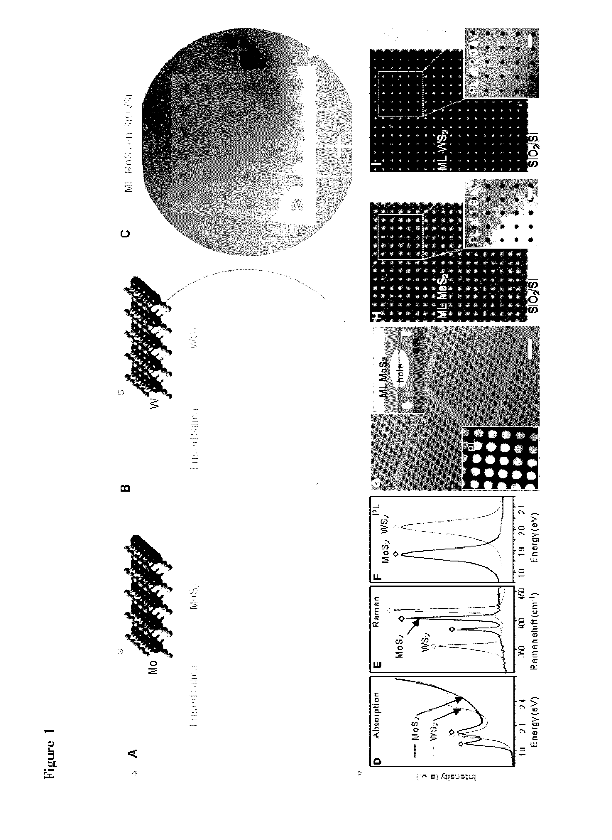
[0059]The growth of semiconducting ML films of MoS2 and WS2 on silicon oxide on a 4-inch wafer scale is described, with both desirable electrical performance and structural continuity, maintained uniformly over the entire films. FIG. 1 shows continuous TMD ML films and shows their wafer-scale homogeneity and intrinsic optical properties. The photos of MoS2 (FIG. 1a; grey) and WS2 (FIG. 1b; light grey) films grown on a transparent 4-inch fused silica wafer show that the TMD grown region (right half) is uniform over the whole substrate and clearly distinguishable from the bare silica substrate (left half). The optical absorption, photoluminescence (PL), and Raman spectra measured from our films show characteristics unique to ML MoS2 and WS2, respectively (FIG. 1d-f). All of these measured spectra have the same peak positions as in exfoliated ML samples (denoted by diamonds), regardless...


PUM

PropertyMeasurementUnit
pressureaaaaaaaaaa
pressureaaaaaaaaaa
grain sizeaaaaaaaaaa

Abstract

Metal-chalcogenide films disposed on a substrate comprising at least one monolayer (e.g., 1 to 10 monolayers) of a metal-chalcogenide. The films can be continuous (e.g., structurally and/or electrically continuous) over 80% or greater of the substrate that is covered by the film. The films can be made by methods based on low metal precursor concentration relative to the concentration of chalcogenide precursor. The methods can be carried out at low water concentration. The films can be used in devices (e.g., electrical devices and electronic devices).

Description

CROSS-REFERENCE TO RELATED APPLICATIONS[0001]This application claims priority to U.S. provisional patent application No. 62 / 148,387, filed Apr. 16, 2015, the disclosure of which is incorporated herein by reference.STATEMENT REGARDING FEDERALLY SPONSORED RESEARCH[0002]This invention was made with government support under contract nos. FA2386-13-1-4118 and FA9550-11-1-0033 awarded by the Air Force Office of Scientific Research and contract nos. DMR-1120296 and ECS-0335765 awarded by National Science Foundation. The government has certain rights in the invention.FIELD OF THE DISCLOSURE[0003]The present disclosure generally relates to metal-chalcogenide films. More particularly, the present disclosure relates to semiconducting metal-chalcogenide films.SUMMARY OF THE DISCLOSURE[0004]In an aspect, the present disclosure provides metal-chalcogenide films (also referred to herein as metal-dichalcogenide films). The films can have one or more metal and / or one or more chalcogenide. The films ...

Claims


Application Information

Patent Timeline
Patent Type & Authority Applications(United States)
IPC IPC(8): H01L29/24H01L29/66H01L21/02H01L29/786
CPCH01L29/24H01L29/786H01L21/0262H01L21/02568H01L29/66969C23C16/305C23C16/52C30B25/00C30B29/46H01L21/02381H01L21/0242H01L21/02422H01L21/02488H01L21/0228H01L21/02417H01L21/02485H01L21/02491H01L21/02499H01L21/28556
Inventor PARK, JIWOONGKANG, KIBUMXIE, SAIEN
Owner CORNELL UNIVERSITY
Why Eureka
Try Eureka