Radiation detector, array of radiation detectors and method for manufacturing a radiation detector

a radiation detector and array technology, applied in the direction of measuring devices, scientific instruments, instruments, etc., can solve the problems of insufficient thermal conductance to achieve a good performance, the boundary of lithography could be quickly reached, and the membrane is poorly thermally insulated from the substrate, so as to achieve the effect of reducing the area consumption of such a ridge and increasing the yield of membrane area

Active Publication Date: 2016-11-03
FRAUNHOFER GESELLSCHAFT ZUR FOERDERUNG DER ANGEWANDTEN FORSCHUNG EV
View PDF1 Cites 1 Cited by
  • Summary
  • Abstract
  • Description
  • Claims
  • Application Information

AI Technical Summary

Benefits of technology

[0018]According to another embodiment, additionally to the thermal insulation by means of the spacer, a ridge may also be disposed at the membrane. The ridge may further increase the thermal insulation provided that the thermal conductance to be achieved may not be achieved exclusively by means of the spacers. However, compared with a spacer that does not function as a thermal insulator, the area consumption of such a ridge is reduced and therefore the membrane area yield is increased. Further, a conventional second ridge may be omitted as the membrane is only suspended on one spacer.

Problems solved by technology

Generally, the membrane is poorly thermally insulated from the substrate by means of only the suspension on the metal contacts.
In this case, the resulting thermal conductance is not sufficiently small to achieve a good performance, since the contact tubes consist of thick metal coatings due to process and stability reasons and therefore conduct the resulting heat in the membrane relatively well.
However, the problem regarding scaling is that, here, the boundaries of lithography could be quickly reached.
On the other hand, also due to process and stability reasons, the contact holes and upper contact areas cannot be scaled arbitrarily small so that a limit exists here as well.
Due to these problems, especially the ridge areas may use more and more space relative to the pixel size at a set thermal conductance (specified by concept), whereby the effective absorber area is additionally reduced and the performance is heavily decreased.
However, the disadvantage herein is that the ridges and the sensor layer are still in one plane.
Thus, the thermal insulation is limited by the free available pixel area.
Furthermore, the resonator condition is not fulfilled in the region of the suspension of the absorber, having a negative effect on the absorption.
The ridge may further increase the thermal insulation provided that the thermal conductance to be achieved may not be achieved exclusively by means of the spacers.

Method used


Image

  • Radiation detector, array of radiation detectors and method for manufacturing a radiation detector
  • Radiation detector, array of radiation detectors and method for manufacturing a radiation detector
  • Radiation detector, array of radiation detectors and method for manufacturing a radiation detector

Examples


Embodiment Construction

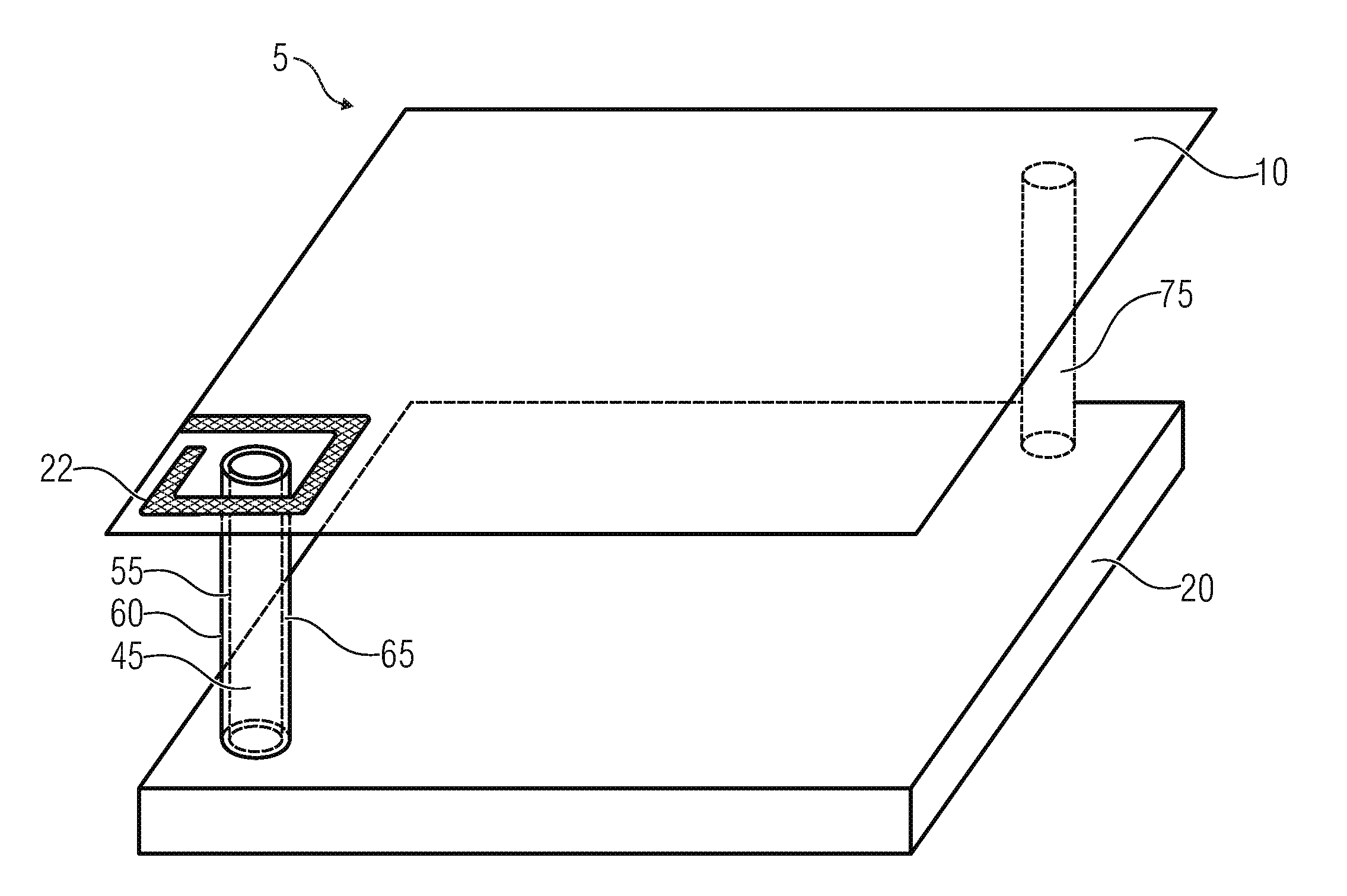
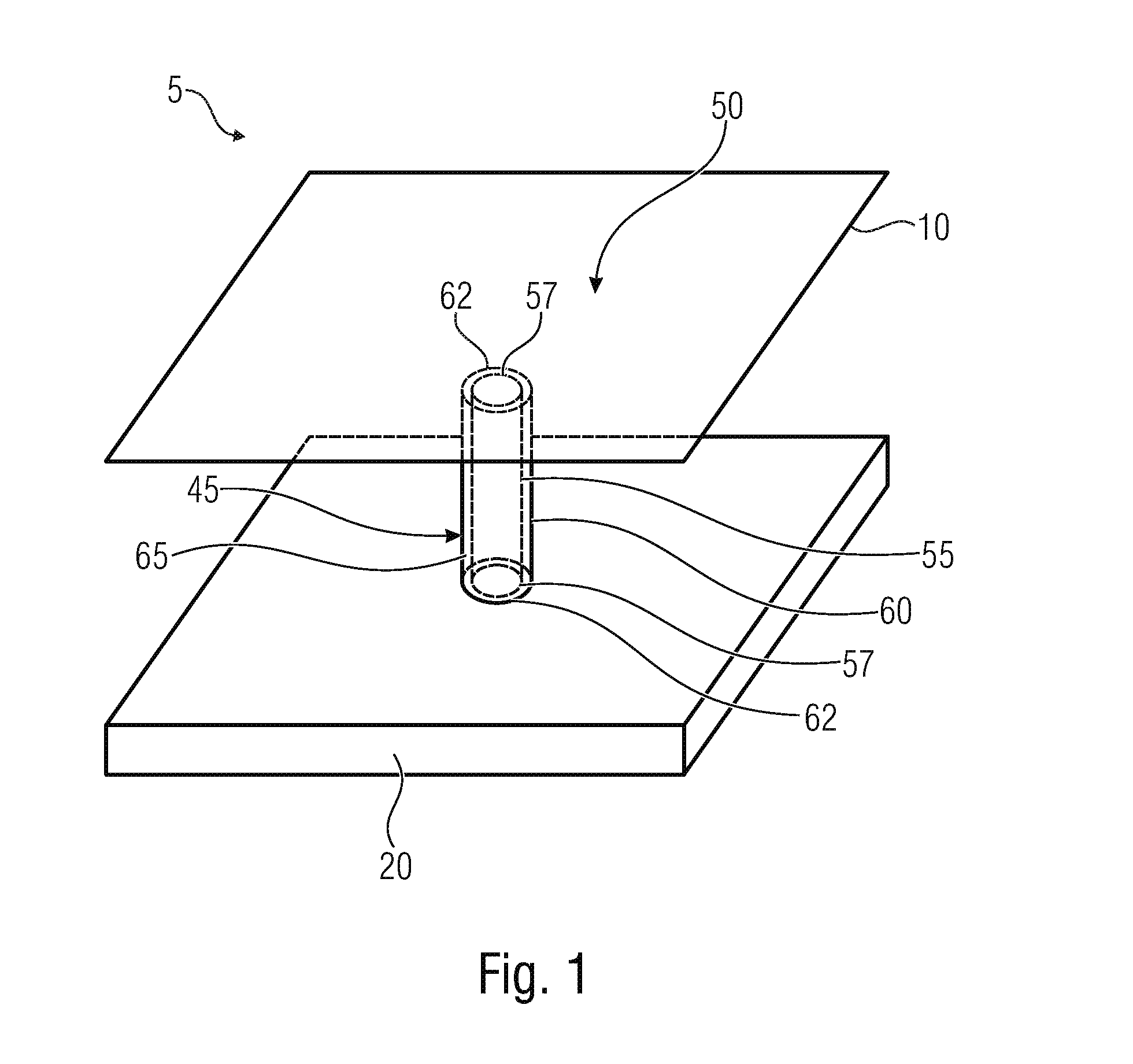
[0040]FIG. 1 shows a schematic illustration of a side view of a radiation detector 5. The radiation detector 5 includes a membrane 10 that is suspended above a substrate 60 by a spacer 45, wherein the spacer 45 thermally insulates a radiation sensor, which is formed in the membrane 10, from the substrate 20. The spacer includes a first layer 55, which is electrically conducting and contacts a first pole 57 of the radiation sensor 50 and of the substrate 20, and further, a second layer 60, which is electrically conducting and electrically insulated from the first electrically conductive layer 55 and contacts a second pole 62 of the radiation sensor 50 and of the substrate 20, which differs in polarity from the first pole 57.

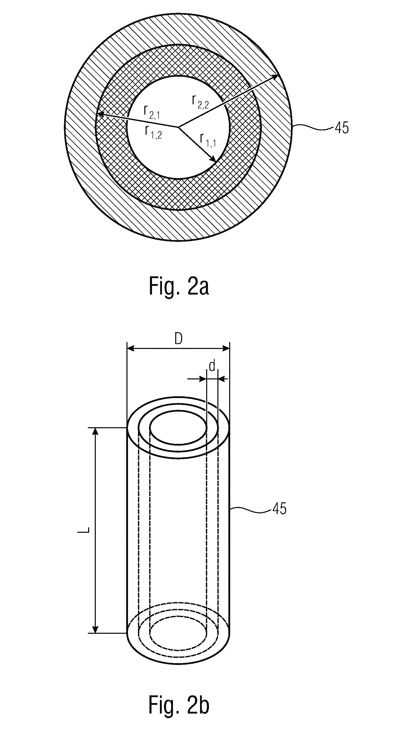
[0041]According to an embodiment, the spacer 45 includes a third layer 65 between the first and the second layer 55 and 60, wherein the third layer 65 electrically insulates the first and second layer 55 and 60 from each another.

[0042]The spacer 45 may realize the...


PUM


Abstract

A radiation detector with a substrate and a membrane, which is suspended above the substrate by a spacer is described, wherein the spacer thermally insulates a radiation sensor, which is formed in the membrane, from the substrate. Further, the spacer includes a first layer, which is electrically conducting and contacts a first pole of the radiation sensor and of the substrate, and a second layer, which is electrically conducting and electrically insulated from the first electrically conductive layer and contacts a second pole of the radiation sensor and of the substrate, wherein the second pole differs in polarity from the first pole.

Description

CROSS-REFERENCE TO RELATED APPLICATIONS[0001]This application claims priority from German Patent Application No. 102015208073.0, which was filed on Apr. 30, 2015, and is incorporated herein in its entirety by reference.BACKGROUND OF THE INVENTION[0002]The present invention relates to a radiation detector, an array of a plurality of radiation detectors and a manufacturing method for manufacturing a radiation detector, wherein the radiation detector may, for example, be a bolometer.[0003]Uncooled resistance microbolometer (hereinafter denoted as microbolometer) arrays may be used for detecting far infrared radiation (8 μm-14 μm) and are also included within the term infrared focal plane arrays (IRFPA). Individual microbolometers, as shown in FIG. 11, may be characterized by a membrane 10, which is suspended in a vacuum over the substrate 20 by two metal contacts 15 by means of thin ridges and is thermally insulated by the ridges 22 (shown in FIG. 12). Essentially the membrane consists...

Claims


Application Information

Patent Timeline
Patent Type & Authority Applications(United States)
IPC IPC(8): G01J5/20
CPCG01J2005/202G01J5/20
Inventor WEILER, DIRKMUCKENSTURM, KAI-MARCELHOCHSCHULZ, FRANK
Owner FRAUNHOFER GESELLSCHAFT ZUR FOERDERUNG DER ANGEWANDTEN FORSCHUNG EV
Why Eureka
Try Eureka