

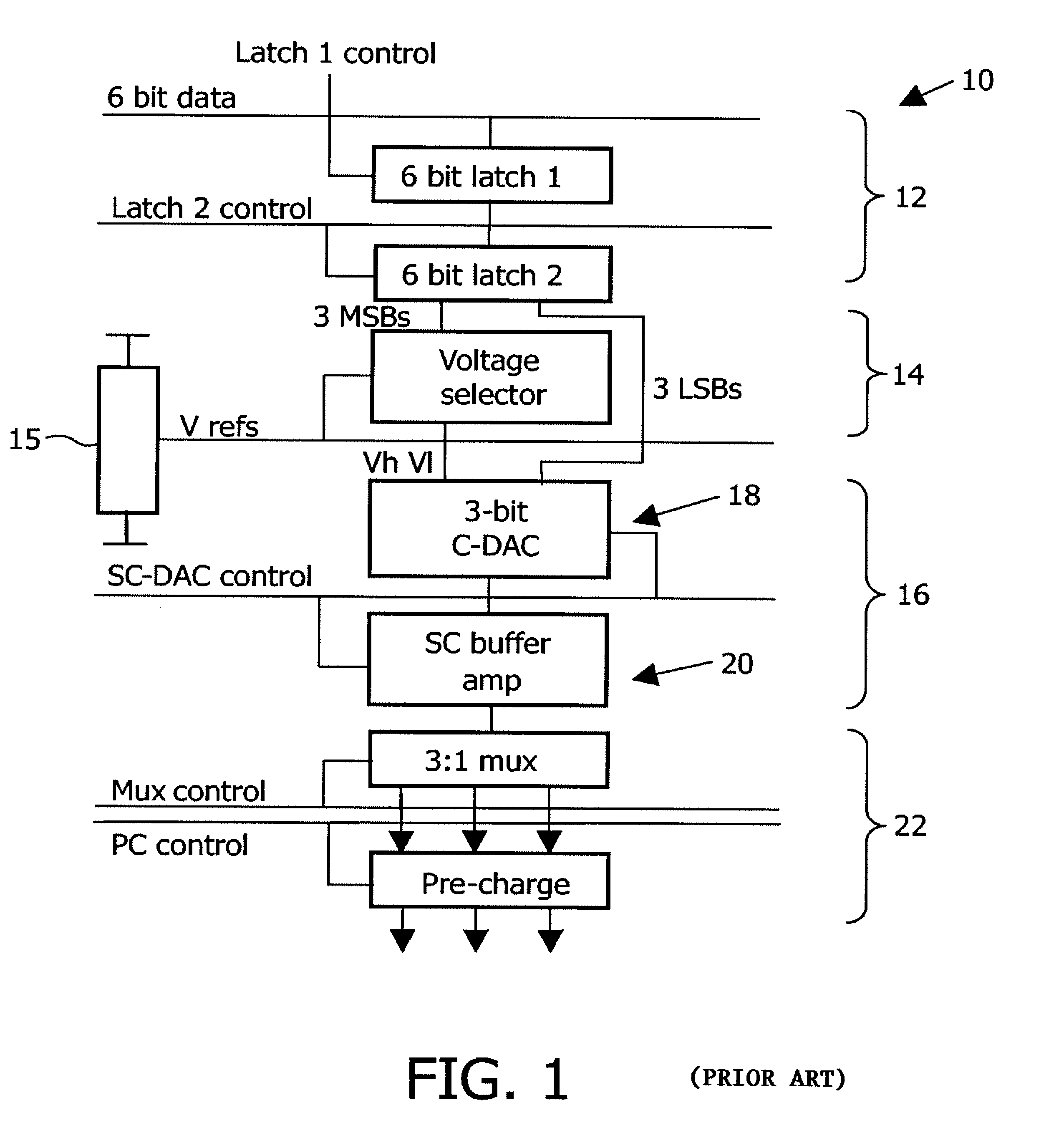
Active matrix array device
a technology of active matrix array and array device, which is applied in the field of active matrix array device, can solve the problems of large layout area using ltps technology, and inability to have a single dac per column, so as to increase the area of each dac, double the time available for setup and active phases, and improve the effect of multiplex ratio
- Summary
- Abstract
- Description
- Claims
- Application Information
AI Technical Summary
Benefits of technology
Problems solved by technology
Method used
Image

Examples
Embodiment Construction
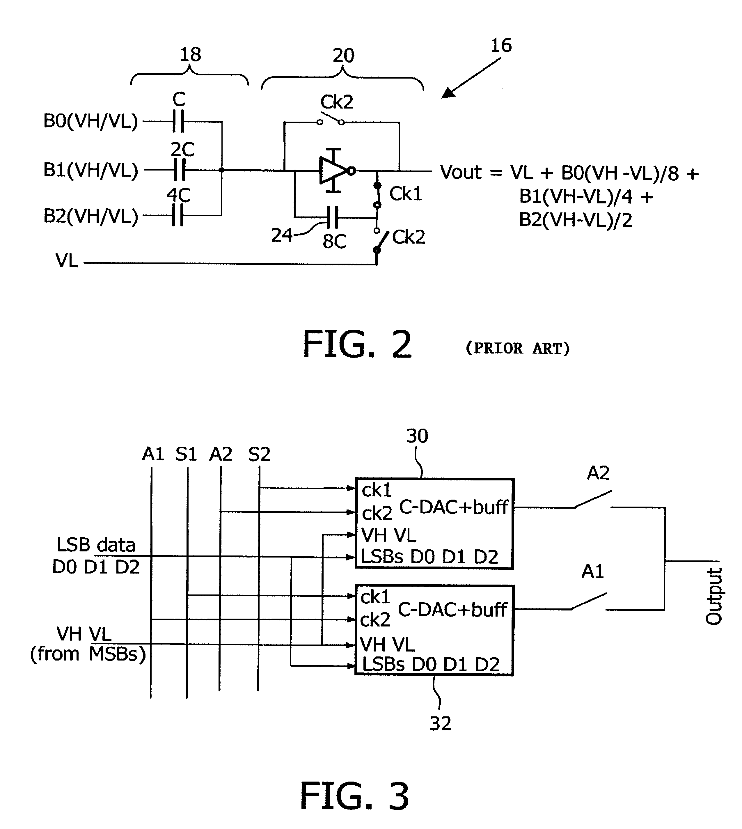
[0064]The invention provides a digital to analogue converter circuit in which a converter arrangement for the least significant bits has first and second digital to analogue converter circuits in parallel and which are adapted to provide an analogue voltage level to the output of the converter arrangement alternately.
[0065]In preferred implementations, each DAC has two switched-capacitor DACs for the least significant bits, and two corresponding buffer amplifiers.
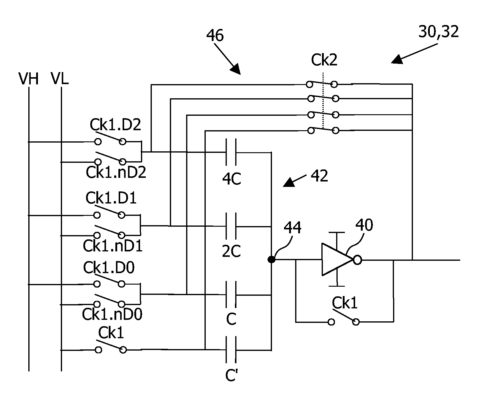
[0066]FIG. 3 shows an example of LSB DAC part of a DAC circuit of the invention.
[0067]FIG. 3 shows the 3 bit LSB data D0, D1, D2 and the voltage rails VH and VL being supplied to the LSB DAC, in the form of first and second digital to analogue converter circuits 30,32 in parallel. These are each implemented as switched capacitor DACs and buffers (“C-DAC+buff”), and they operate in opposite phases. This enables the number of latches and MSB DACs to remain the same.
[0068]As shown in FIG. 3, two clock signals are used to contr...
PUM
 Abstract
Description
Claims
Application Information