
Sensing fiber and sensing device

a sensing fiber and fiber technology, applied in the field of fiber and optical devices, can solve the problems of difficult control of the thickness limited application and sensitivity of the surface plasmon generated by the evanescent wave of the metal film, etc., and achieve the effect of effective transmission and good sensing

Inactive Publication Date: 2016-11-17
I-SHOU UNIVERSITY
View PDF5 Cites 13 Cited by
  • Summary
  • Abstract
  • Description
  • Claims
  • Application Information

AI Technical Summary

Benefits of technology

The invention provides a sensing device that can effectively sense objects using a metal sensing layer with multiple metal grating structures. This ensures that the sensing light is effectively transmitted to the object and the signal light converted by it is obtained, resulting in a good sensing effect. Additionally, the sensing device has a sensing fiber, which allows for all-receiving units to receive a good signal light of the object.

Problems solved by technology

However, application and sensitivity of the surface plasmon generated by the evanescent wave of the metal film is limited, and in the process of forming the metal film in the photonic crystal structure fiber having air holes, the shape of the air holes will be changed under high temperature condition, and it is very difficult to control the quality of the thickness of the metal film.

Method used


Image

  • Sensing fiber and sensing device
  • Sensing fiber and sensing device
  • Sensing fiber and sensing device

Examples


first embodiment

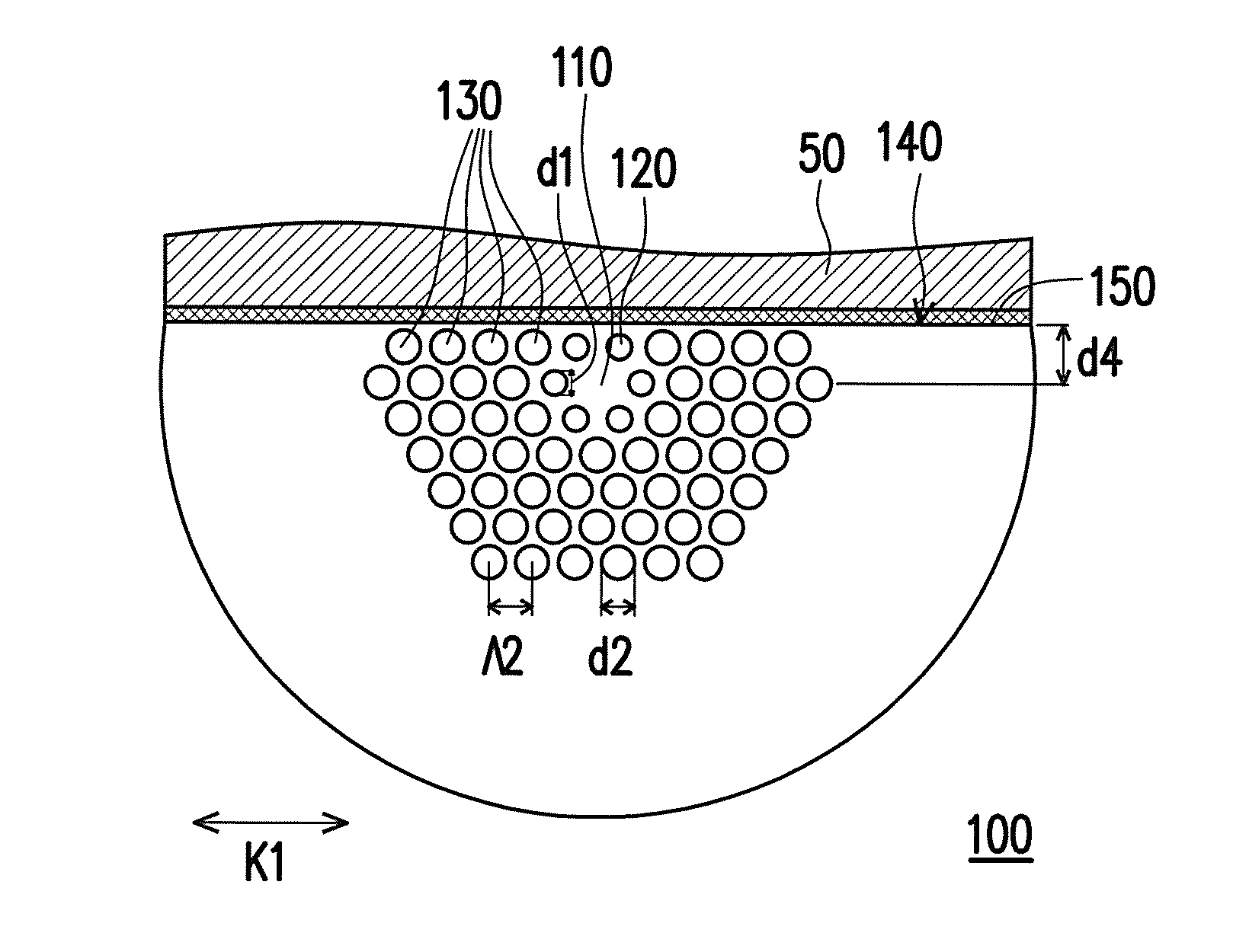
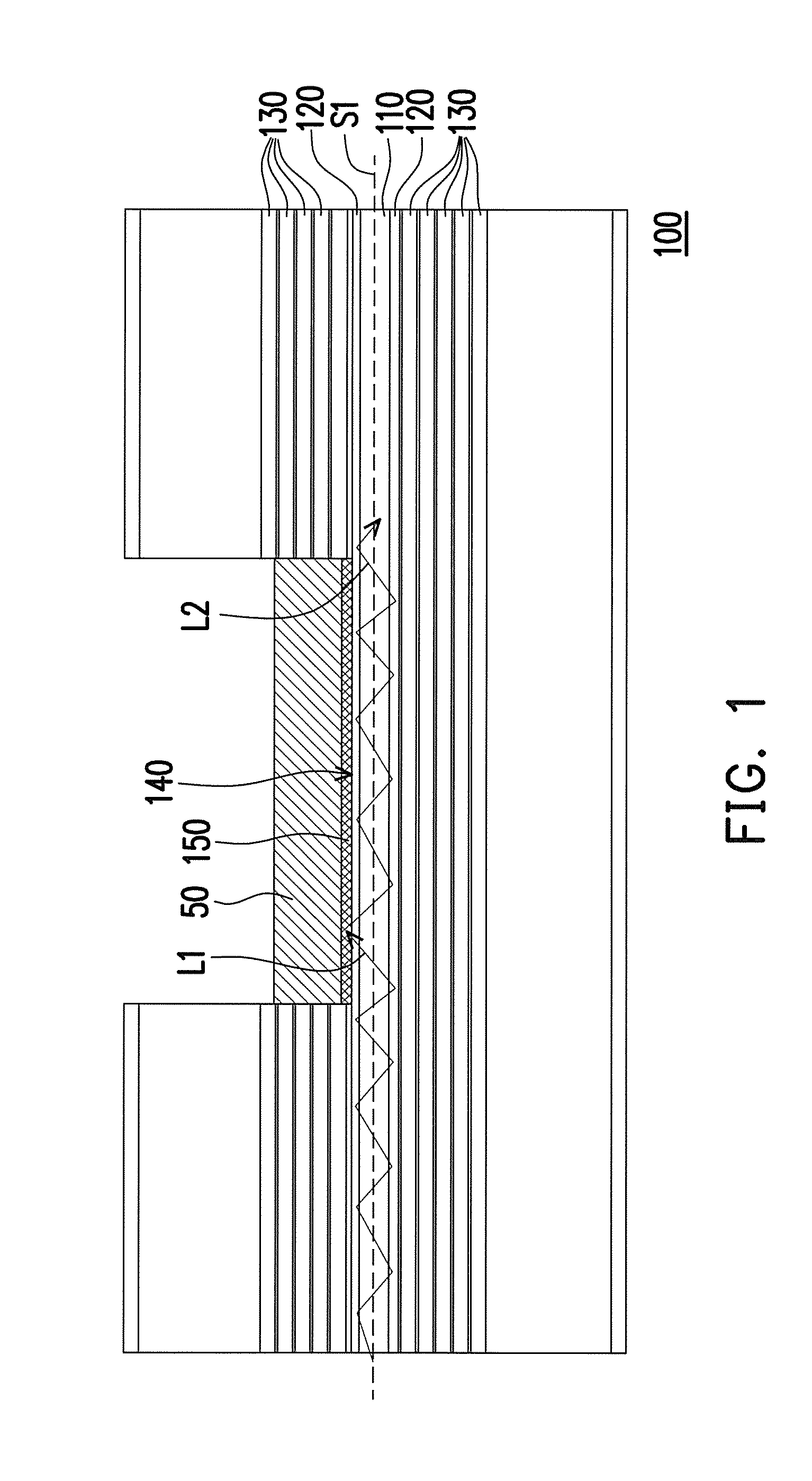
[0032]In the first embodiment, the refractive coefficient of the photonic crystal structures 120 and 130 is smaller than the refractive coefficient of the core 110. Specifically, the refractive coefficient of the photonic crystal structures 120 and 130 ranges from 1.402 to 1.42, and the material of the core 110 is, for example, silica germanium which has the refractive coefficient ranging from 1.437 to 1.44, so that the refractive coefficient of the core is increased to make the sensing light L1 can be easily reflected inside the core 110 by the photonic crystal structures 120 and 130, and to increase the transmission efficiency.

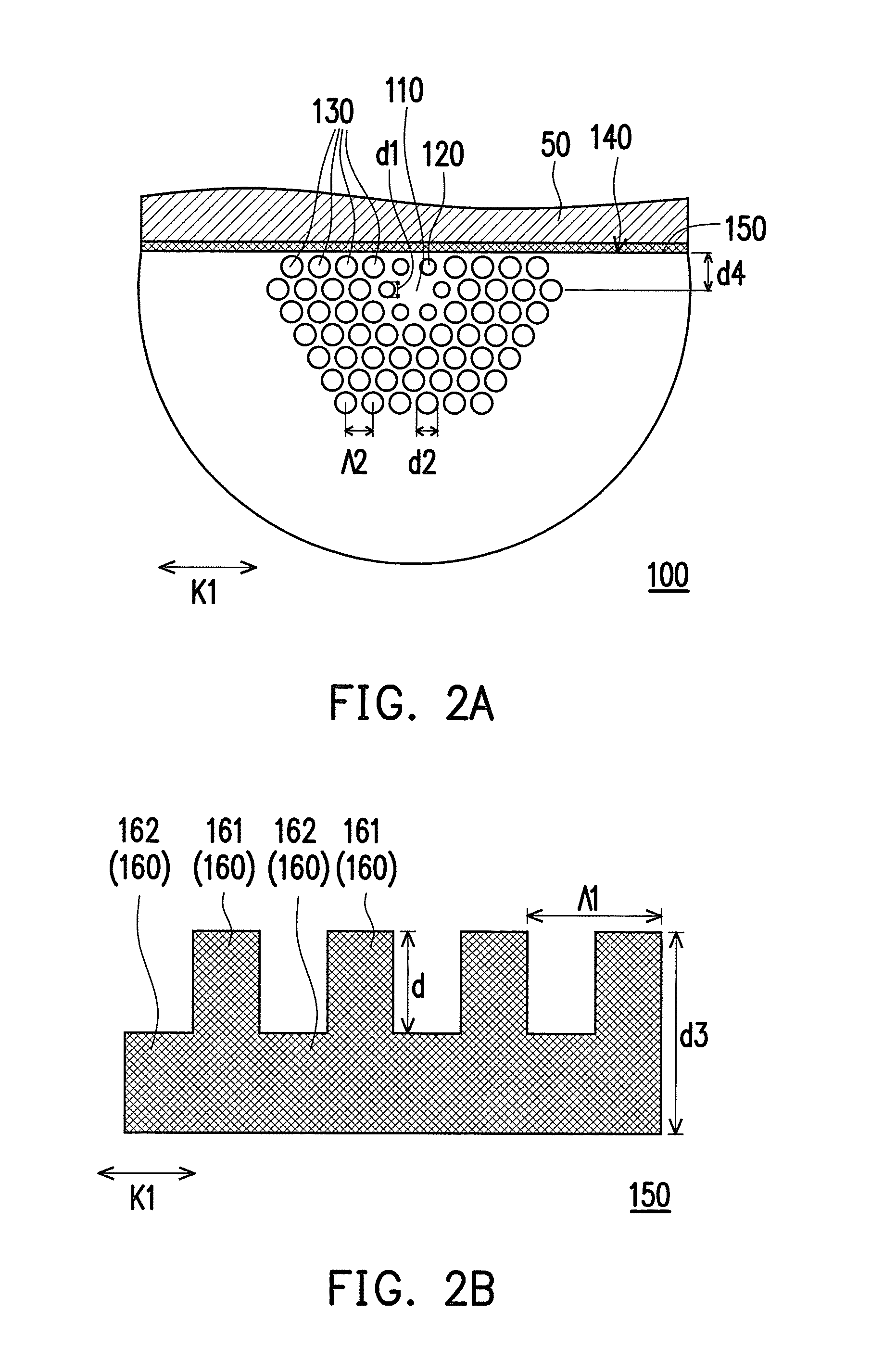
[0033]In the present embodiment, the sensing surface 140 extends along a part of the path S 1 and be adjacent to the core 110. The sensing surface 140 in the present embodiment is, for example, formed by grinding and polishing the complete solid photonic crystal fiber. The metal sensing layer 150 is, for example, a film made by coating metal materials on the...

third embodiment

[0046]Table 1 contains the experimental data of the invention, and FIG. 5A, 5B are graphs according to the experimental data of the metal sensing layer with each period of table 1. The mode real part and the mode imaginary part are calculated by the Lorentz model, and the sensitivity is calculated by the formula

Sλ(nmRIU)=λpeak(na)na,

wherein Sλ is the sensitivity having unit: nm / RIU (RIU is Refractive Index Unit), λpeak is the resonance wavelength when the coupled mode is generated, na is the reflective index of the analyzed object.

TABLE 1data in the coupled mode of 3 types of metal grating periodGrating period102030Period length (μm)3.79331.89661.2644Resonance wavelength (nm)800820850Basic mode real part1.4319441.4314881.430982Basic mode imaginary5.4697438.60670514.77885part (×10−5)Surface plasmon mode1.4313551.4311931.430977real partSurface plasmon mode0.0042470.0045160.003322imaginary partSensitivity (μm / RIU)26.5832.0837.83

[0047]As shown in table 1, when the value of the period in...

fourth embodiment

[0048]Table 2 contains the experimental data of the invention, and FIG. 6A, 6B are graphs according to the experimental data of the metal sensing layer with each period of table 2. The mode real part and the mode imaginary part are calculated by the Lorentz model, and the sensitivity is calculated by the formula

Sλ(nmRIU)=λpeak(na)na,

wherein Sλ is the sensitivity having unit: nm / RIU (RIU is Refractive Index Unit), λpeak is the resonance wavelength when the coupled mode is generated, na is the reflective index of the analyzed object.

TABLE 2data in the coupled mode of 3 types of metal gratingGrating metal materialsAgAg—CuAg—AuPeriod length (μm)1.2644Resonance wavelength (nm)850850875Basic modal real part1.430921.431011.430443Basic modal imaginary part14.7788513.3449613.69802(×10−5)Surface plasmon mode1.4309771.4300741.430214real partSurface plasmon mode0.0033220.003560.003705imaginary partSensitivity (μm / RIU)37.8337.8340.71

[0049]In detail, FIG. 6A is a diagram about equivalent refracti...


PUM

PropertyMeasurementUnit
total thicknessaaaaaaaaaa
total thickness d3aaaaaaaaaa
thicknessaaaaaaaaaa

Abstract

A sensing fiber adapted to transmit a sensing light along a path and sense an object is provided. The fiber includes a core, a plurality of photonic crystal structures surrounding the core, a sensing surface and a metal sensing layer. The core is located at the center of the fiber. The photonic crystal structures extend along the path. The sensing surface extends along part of the path and adjacent to the core, and the metal sensing layer having a plurality of metal grating structure is disposed on the sensing surface. When the fiber is sensing the object, the metal sensing layer is located between the sensing surface and the object, and part of the sensing light will be converted into a signal light by the object on the metal sensor layer. A sensing device is also provided.

Description

CROSS REFERENCE TO RELATED APPLICATION[0001]This application claims the priority benefit of Taiwan application serial no. 104115562, filed on May 15, 2015. The entirety of the above-mentioned patent application is hereby incorporated by reference herein and made a part of specification.BACKGROUND OF THE INVENTION[0002]1. Field of the Invention[0003]The invention relates to a fiber and an optical device, specifically to a sensing fiber and a sensing device.[0004]2. Description of Related Art[0005]Along with the development of science and technology, infoimation transfer has become one of the most promising science and technology to be developed. The capacity, stability, quality, and speed of infoll iation transmission always are the main topics of infoi nation transfer science and technology, so that the important role and the future development of the optical fiber communication are further highlighted and emphasized. In 1987, the two scientists Sajeev John and Eli Yablonovitch sepa...

Claims


Application Information

Patent Timeline
Patent Type & Authority Applications(United States)
IPC IPC(8): G01N21/552G01N33/543G02B6/02G01N21/65G01N21/64
CPCG01N21/554G01N21/658G01N21/648G01N2201/061G01N33/54373G01N2201/088G01N2201/068G02B6/02314G02B6/02347
Inventor CHIANG, JUNG-SHENGSUN, NAI-HSIANGLIU, WEN-FUNGLIN, SHIH-CHIANG
Owner I-SHOU UNIVERSITY
Learn More