Semiconductor structure and process thereof

Inactive Publication Date: 2016-11-17
UNITED MICROELECTRONICS CORP
View PDF5 Cites 8 Cited by
  • Summary
  • Abstract
  • Description
  • Claims
  • Application Information

AI Technical Summary

Benefits of technology

[0008]According to the above, the present invention provides a semiconductor structure and process thereof, which forms a dielectric layer having a recess on a substrate, forms a barrier layer to cover the recess, forms a conductive layer on the barrier layer by an atomic layer deposition (ALD) process, and then pulls down sidewall parts of the conductive layer, thereby the conductive layer can be entirely covered by a conductive material filling the recess. As a result, the conductive layer can avoid being damaged or polished by processes such as a planarization process later performed on the conductive material and the barrier layer for forming a plug. Therefore, the galvanic corrosion between the barrier layer and the conductive layer can be avoided by selecting the forming process of the conductive material, which can make the equilibrium potential difference between the barrier layer and the conductive layer be different from the equilibrium potential difference between the barrier layer and the conductive material.

Problems solved by technology

As the miniaturization of semiconductor devices increases, filling the barrier layer and the low resistivity into a contact hole has become an important issue to form the contact plug and maintaining or enhancing the performances of formed semiconductor devices as well.

Method used


Image

  • Semiconductor structure and process thereof
  • Semiconductor structure and process thereof
  • Semiconductor structure and process thereof

Examples


Embodiment Construction

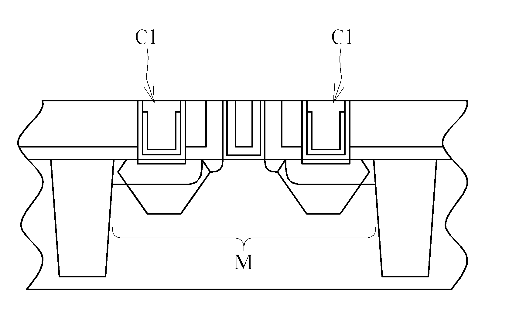
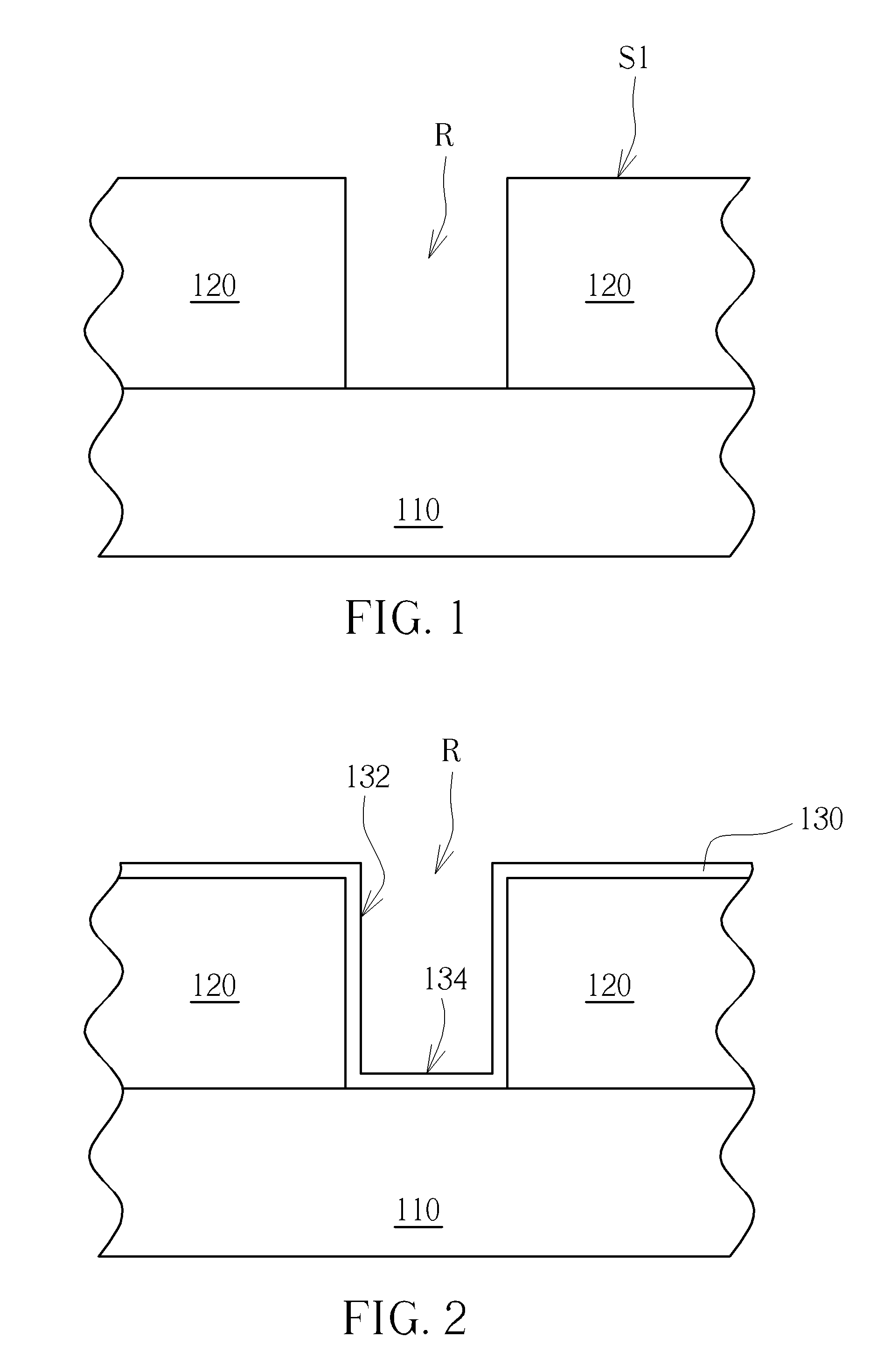
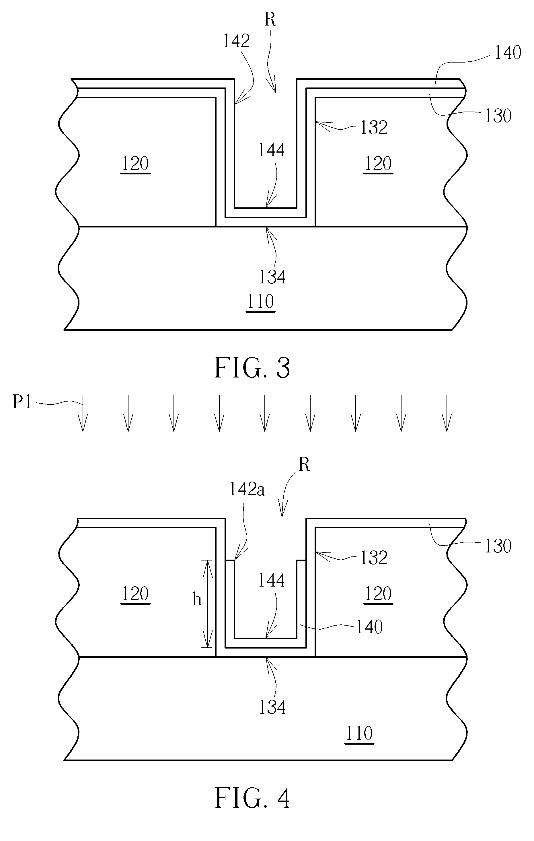
[0014]FIGS. 1-6 schematically depict cross-sectional views of a semiconductor process according to an embodiment of the present invention. As shown in FIG. 1, a substrate 110 is provided. The substrate 110 may be a semiconductor substrate such as a silicon substrate, a silicon containing substrate, a III-V group-on-silicon (such as GaN-on-silicon) substrate, a graphene-on-silicon substrate or a silicon-on-insulator (SOI) substrate. A dielectric layer 120 having a recess R is formed on the substrate 110. More precisely, a dielectric material (not shown) may blanketly cover the substrate 110; the dielectric material is planarized to form the dielectric layer 120 having a flat top surface S1; and then, the dielectric layer 120 is etched by a dry etching process or / and a wet etching process to form the recess R in the dielectric layer 120 and expose the substrate 110, but it is not restricted thereto. The dielectric layer 120 may be an inter-level dielectric layer, which may be an oxide...


PUM


Abstract

A semiconductor process includes the following steps. A dielectric layer having a recess is formed on a substrate. A barrier layer is formed to cover the recess, thereby the barrier layer having two sidewall parts. A conductive layer is formed on the barrier layer by an atomic layer deposition process, thereby the conductive layer having two sidewall parts. The two sidewall parts of the conductive layer are pulled down. A conductive material fills the recess and has a part contacting the two sidewall parts of the barrier layer protruding from the two sidewall parts of the conductive layer, wherein the equilibrium potential difference between the barrier layer and the conductive layer is different from the equilibrium potential difference between the barrier layer and the conductive material. Moreover, the present invention also provides a semiconductor structure formed by said semiconductor process.

Description

BACKGROUND OF THE INVENTION[0001]1. Field of the Invention[0002]The present invention relates generally to a semiconductor structure and process thereof, and more specifically to a semiconductor structure including plugs and process thereof.[0003]2. Description of the Prior Art[0004]Field effect transistors are important electronic devices in the fabrication of integrated circuits, and as the size of the semiconductor device becomes smaller and smaller, the fabrication of the transistors also improves and is constantly enhanced for fabricating transistors with smaller sizes and higher quality. In the conventional method of fabricating transistors, agate structure is first formed on a substrate, and a lightly doped drain (LDD) is formed on the two corresponding sides of the gate structure. Next, a spacer is formed on the sidewall of the gate structure and an ion implantation process is performed to forma source / drain region within the substrate by utilizing the gate structure and spa...

Claims


Application Information

Patent Timeline
Patent Type & Authority Applications(United States)
IPC IPC(8): H01L23/535H01L21/768H01L23/532
CPCH01L23/535H01L23/53266H01L21/76895H01L21/7684H01L21/76843H01L21/28088H01L21/28556H01L21/28562H01L21/76865H01L21/76874H01L23/485H01L29/66545H01L29/7833
Inventor LI, KUN-JUHUANG, SHU MINHUNG, KUO-CHINHUANG, PO-CHENGLI, YU-TINGLEE, PEI-YUTSAI, MIN-CHUANLIN, CHIH-HSUNSIE, WU-SIANLIN, JEN-CHIEH
Owner UNITED MICROELECTRONICS CORP
Why Eureka
Try Eureka