Encapsulating film stacks for OLED applications

a technology of encapsulation and film stack, which is applied in the direction of basic electric elements, electrical equipment, semiconductor devices, etc., can solve the problems of increasing drive voltage, reducing electroluminescence efficiency, and limited life of oled structures, so as to achieve desired optical properties and film transparency, improve the barrier performance of tfe structures

Active Publication Date: 2016-11-17
APPLIED MATERIALS INC
View PDF1 Cites 14 Cited by
  • Summary
  • Abstract
  • Description
  • Claims
  • Application Information

AI Technical Summary

Benefits of technology

[0009]Embodiments described herein generally relate to a method and apparatus for encapsulating an OLED structure, more particularly, to a TFE structure for an OLED structure. The TFE structure includes at least one dielectric layer and at least two barrier layers, and the TFE structure is form...

Problems solved by technology

OLED structures may have a limited lifetime, characterized by a decrease in electroluminescence efficiency and an increase in drive voltage.
However, different materials, especially organic and inorganic materials, often have different film properties, thereby resulting in poor surface adhesion at the interface where the organic and the inorganic layers are in contact with.
Poor interface adhesion ofte...

Method used


Image

  • Encapsulating film stacks for OLED applications
  • Encapsulating film stacks for OLED applications
  • Encapsulating film stacks for OLED applications

Examples


Embodiment Construction

[0027]Embodiments described herein generally relate to a method and apparatus for encapsulating an OLED structure, more particularly, for manufacturing a TFE structure for encapsulating an OLED structure. The TFE structure includes at least one dielectric layer and at least two barrier layers, and the TFE structure is formed over the OLED structure. The at least one dielectric layer is deposited by atomic layer deposition (ALD). The dielectric layer formed by ALD process has desired film properties, such as relatively high film density as well as strong atomic bonding structures so that good moisture resistance, desired optical properties and the barrier performance of the TFE structure may be obtained and improved.

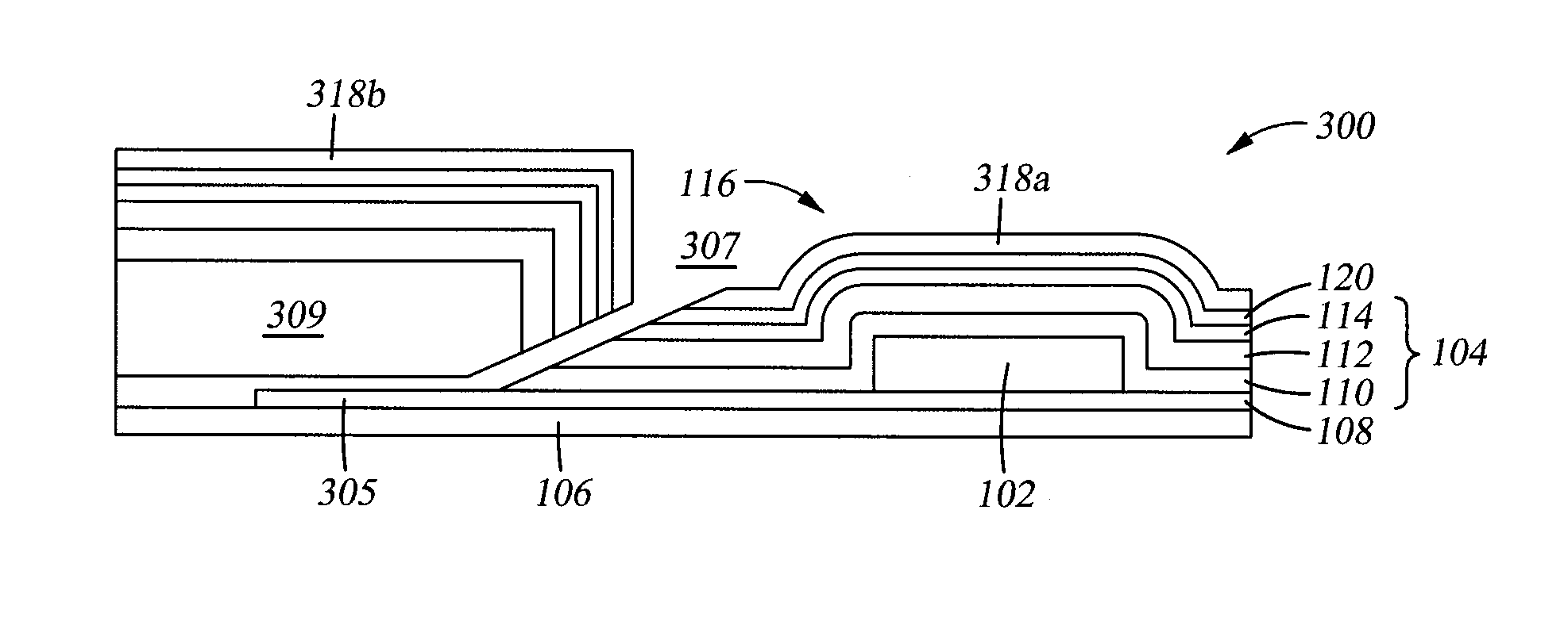
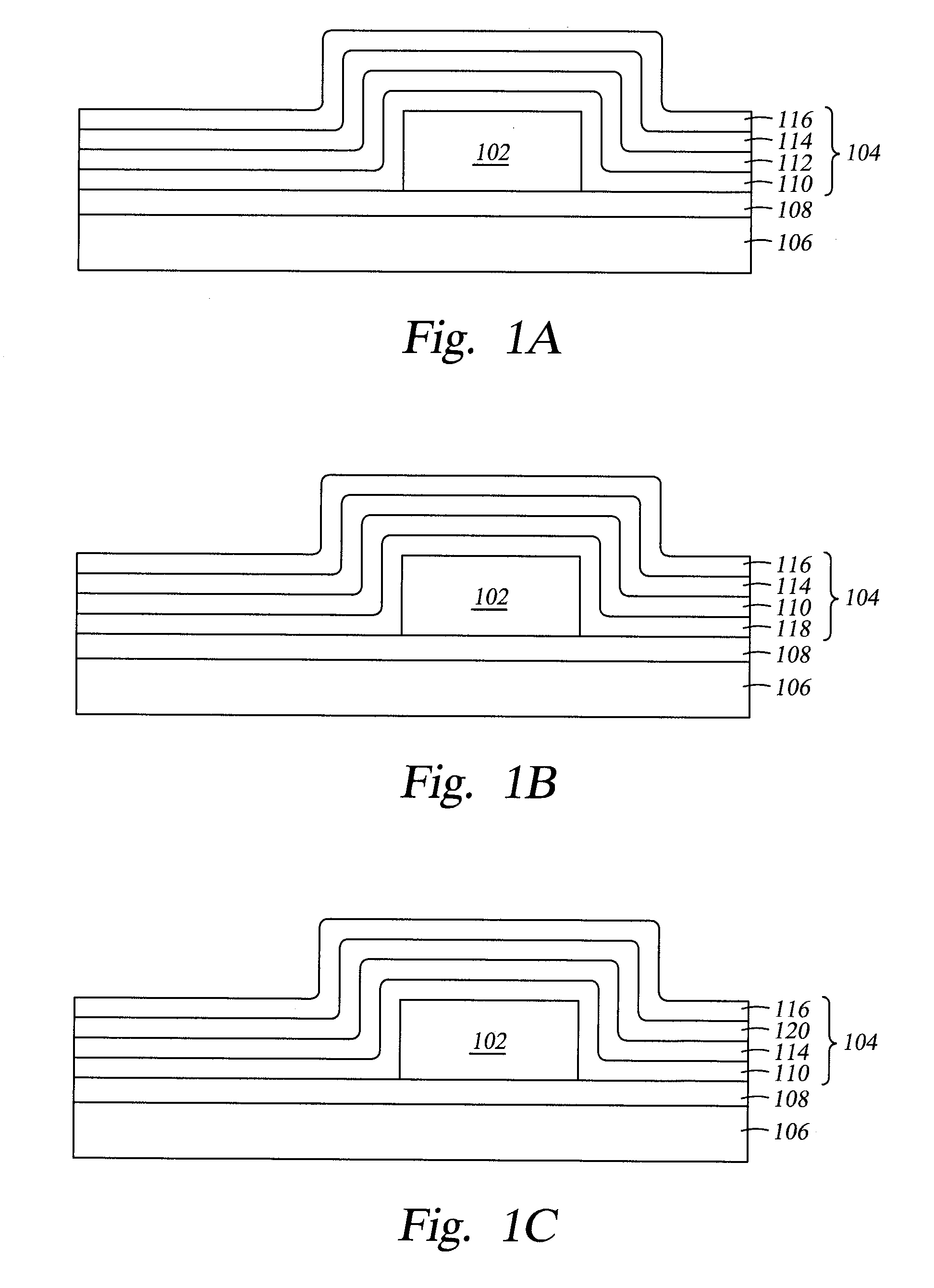
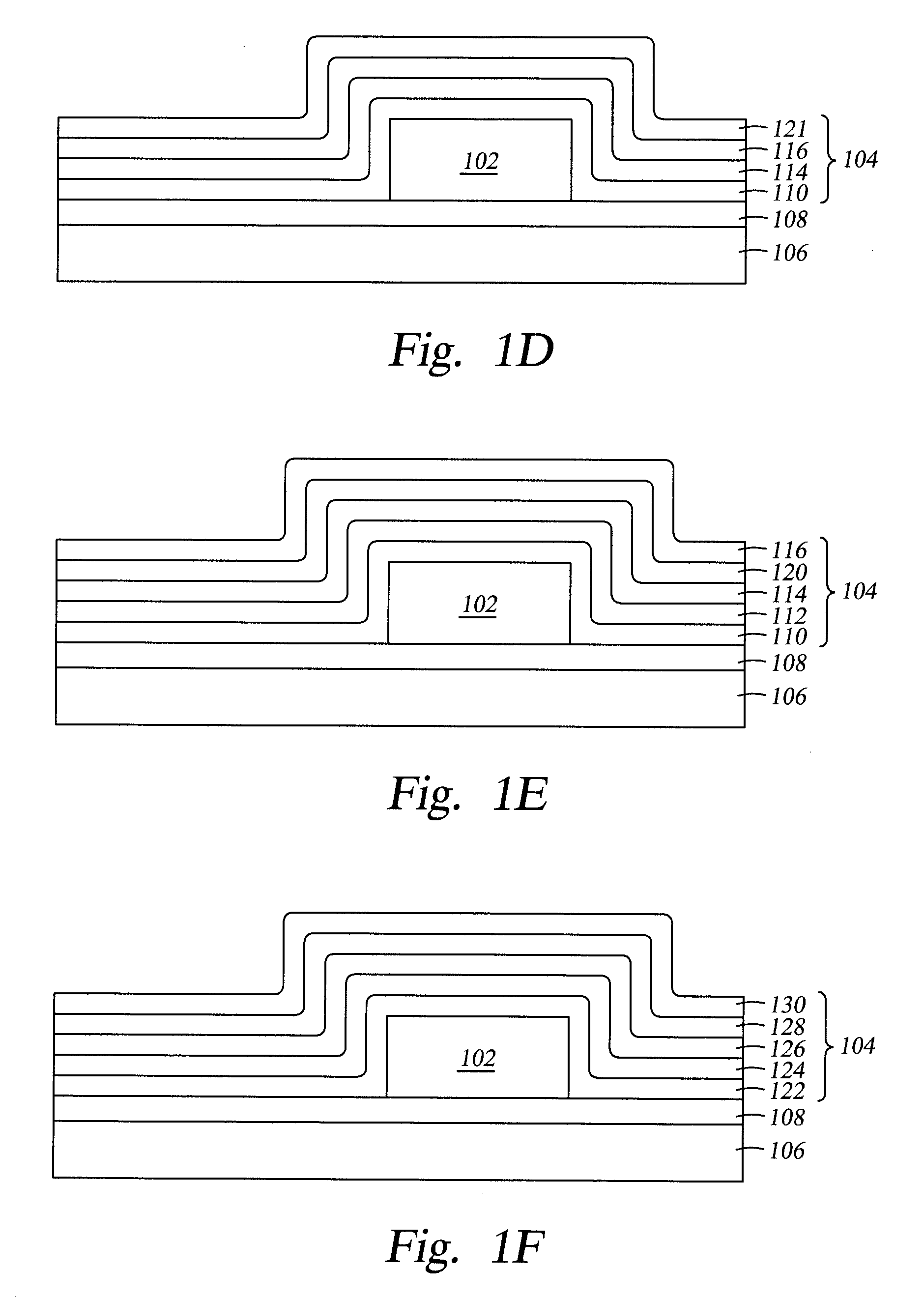
[0028]FIGS. 1A-1F are schematic cross sectional views of an OLED structure 102 encapsulated by a TFE structure 104 according to various embodiments described herein. As shown in FIG. 1A, the OLED structure 102 may be disposed over a substrate 106, and a contact layer 108 ...


PUM


Abstract

Embodiments described herein generally relate to a method and apparatus for encapsulating an OLED structure, more particularly, to a TFE structure for an OLED structure. The TFE structure includes at least one dielectric layer and at least two barrier layers, and the TFE structure is formed over the OLED structure. The at least one dielectric layer is deposited by atomic layer deposition (ALD). Having the at least one dielectric layer formed by ALD in the TFE structure improves the barrier performance of the TFE structure.

Description

CROSS-REFERENCE TO RELATED APPLICATIONS[0001]This application claims benefit of U.S. Provisional Application Ser. No. 62 / 161,760 filed May 14, 2015 (Attorney Docket No. APPM / 22915L) and U.S. Provisional Application Ser. No. 62 / 172,784 filed Jun. 8, 2015 (Attorney Docket No. APPM / 22915L02), which is incorporated by reference in its entirety.BACKGROUND[0002]1. Field[0003]Embodiments described herein generally relate to a method and apparatus for encapsulating an organic light emitting diode (OLED) structure, more particularly, to a thin film encapsulation (TFE) structure for an OLED structure.[0004]2. Description of the Related Art[0005]Organic light emitting diode displays (OLED) have gained significant interest recently in display applications in view of their faster response times, larger viewing angles, higher contrast, lighter weight, lower power and amenability to flexible substrates. Generally, a conventional OLED is enabled by using one or more layers of organic materials sand...

Claims


Application Information

Patent Timeline
IPC IPC(8): H01L51/52H01L21/67H01L51/56
CPCH01L51/5256H01L21/67207H01L51/56H01L21/67167H01L21/6719H01L21/67742H01L21/68742H01L21/68785H01L21/68792H10K59/8731H10K50/8445
Inventor CHEN, JRJYAN JERRYRUI, XIANGXINCHOI, SOO YOUNG
Owner APPLIED MATERIALS INC
Why Eureka
Try Eureka