Deposition apparatus, apparatus for successive deposition, and method for manufacturing semiconductor device

a semiconductor device and deposition apparatus technology, applied in the direction of semiconductor/solid-state device testing/measurement, vacuum evaporation coating, coating, etc., can solve the problems of high cost in designing a clean room and limit the layout of the clean room, and achieve high reliability, stable electric characteristics, and high reliability. the effect of semiconductor devices

Inactive Publication Date: 2016-11-24
SEMICON ENERGY LAB CO LTD
View PDF3 Cites 1 Cited by
  • Summary
  • Abstract
  • Description
  • Claims
  • Application Information

AI Technical Summary

Benefits of technology

[0010]Further, along with the above increase in the size of a substrate, the size of a deposition apparatus has been increased. However, a deposition apparatus having a large floor area (so-called footprint) causes a problem of high cost in designing of a clean room as well as limitation on the layout of the clean room.
[0061]According to one embodiment of the present invention, a deposition apparatus with which a semiconductor device having stable electric characteristics and high reliability is realized can be provided. A deposition apparatus which enables mass production of highly reliable semiconductor devices with the use of a large-sized substrate such as a mother glass can be provided. A method for manufacturing a semiconductor device having stable electric characteristics and high reliability can be provided.

Problems solved by technology

However, a deposition apparatus having a large floor area (so-called footprint) causes a problem of high cost in designing of a clean room as well as limitation on the layout of the clean room.

Method used


Image

  • Deposition apparatus, apparatus for successive deposition, and method for manufacturing semiconductor device
  • Deposition apparatus, apparatus for successive deposition, and method for manufacturing semiconductor device
  • Deposition apparatus, apparatus for successive deposition, and method for manufacturing semiconductor device

Examples


modification example 1

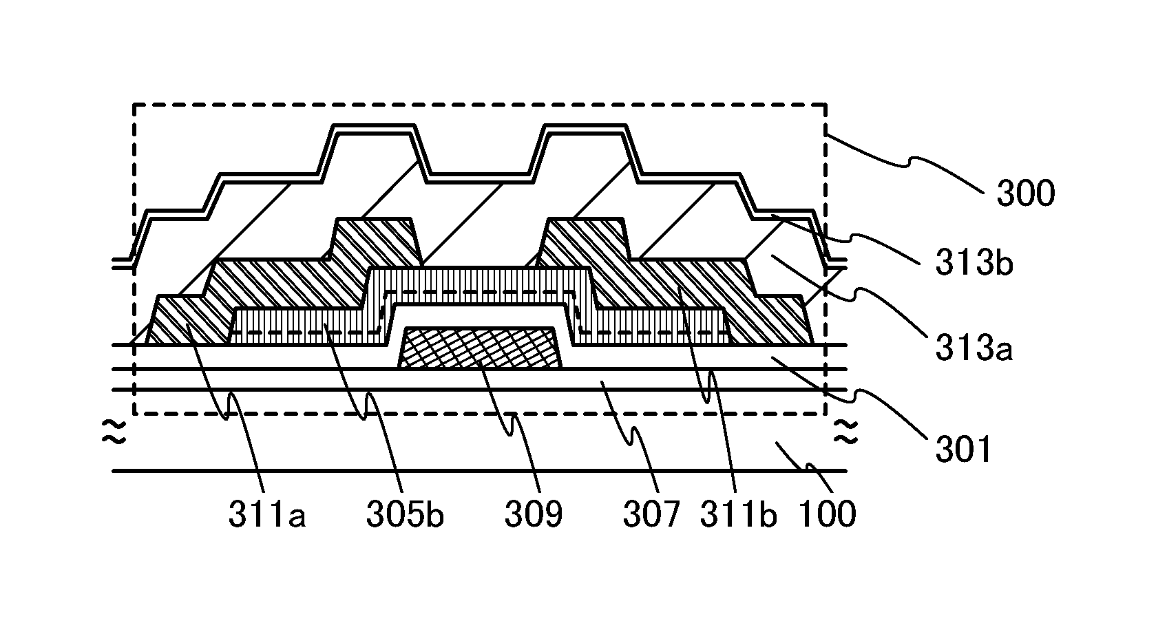
[0176]A method for forming an oxide insulating layer 211, an oxide insulating layer 213b, and an oxide semiconductor layer 215a having c-axis-aligned crystallinity, which are illustrated in FIG. 5A, over the substrate 100 will be described.

[0177]Steps up to and including the step of performing the first heat treatment in the first heating chamber 121 are performed in a manner similar to that of the foregoing example. In other words, the oxide insulating layer 211 is formed in the first deposition chamber 111, an oxide film is formed over the oxide insulating layer in the second deposition chamber 112, and the first heat treatment is performed in the first heating chamber 121. By the first heat treatment, a lower layer of the oxide film becomes the oxide insulating layer 213b and an upper layer thereof becomes an oxide semiconductor layer having c-axis aligned crystallinity.

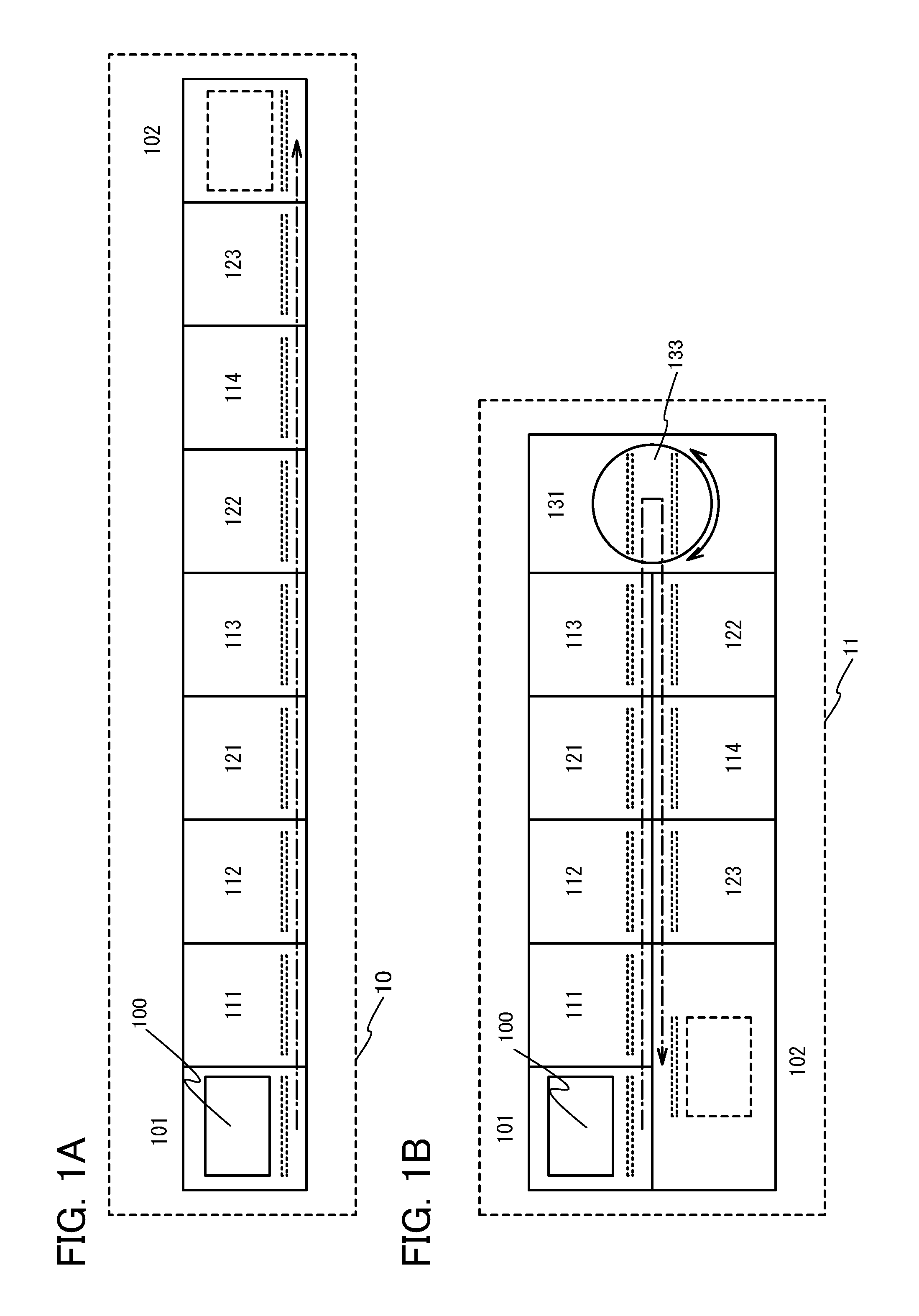
[0178]Next, in the third deposition chamber 113, an oxide semiconductor film is formed while the substrate 100 ...

modification example 2

[0182]A method for forming an oxide insulating layer 221 and an oxide semiconductor layer 221a having c-axis alignment, which are illustrated in FIG. 5B, over the substrate 100 will be described.

[0183]First, the substrate is transferred from the load chamber 101 to the first deposition chamber 111, and the oxide insulating layer 221 is formed. After that, the substrate is only transferred through the second deposition chamber 112 without being processed therein. Then, the substrate is carried into the first heating chamber 121 and first heat treatment is performed. By the first heat treatment, impurities such as hydrogen, water, and a hydroxyl group in the oxide insulating layer 221 can be removed. Note that it is also possible for second heat treatment performed later to serve as the first heat treatment, without performing the first heat treatment.

[0184]Then, in the third deposition chamber 113, a first oxide semiconductor film having a thickness greater than or equal to 1 nm and ...

modification example 3

[0190]A method for forming an oxide insulating layer 231 and an oxide semiconductor layer 234, which are illustrated in FIG. 5C, over the substrate 100 will be described.

[0191]First, the substrate 100 is transferred from the load chamber 101 to the first deposition chamber 111, and the oxide insulating layer 231 is formed. As the oxide insulating layer 231, for example, a 100-nm-thick silicon oxide film is formed by a sputtering method.

[0192]Then, the substrate is only transferred through the second deposition chamber 112 without being processed therein, and first heat treatment is performed in the first heating chamber 121. By the first heat treatment, impurities such as hydrogen, water, and a hydroxyl group in the oxide insulating layer 231 can be removed. Note that it is also possible for second heat treatment performed later to serve as the first heat treatment, without performing the first heat treatment.

[0193]Next, the substrate is transferred to the third deposition chamber 1...


PUM

PropertyMeasurementUnit
angleaaaaaaaaaa
sizeaaaaaaaaaa
sizeaaaaaaaaaa

Abstract

An oxide semiconductor layer is formed with a deposition apparatus including a transfer mechanism for a substrate, a first deposition chamber in which an oxide semiconductor is deposited, and a first heating chamber in which first heat treatment is performed. The first deposition chamber and the first heating chamber are sequentially provided along a path of the substrate transferred by the transfer mechanism. The substrate is held so that an angle formed by a deposition surface of the substrate and the vertical direction is in a range of greater than or equal to 1° and less than or equal to 30°. Without exposure to the air, the first heat treatment can be performed after a first film is formed over the substrate.

Description

BACKGROUND OF THE INVENTION1. Field of the Invention[0001]The present invention relates to a deposition apparatus and an apparatus for successive deposition. The present invention relates to a method for manufacturing a semiconductor device.[0002]Note that a semiconductor device in this specification and the like refers to all devices which can function by utilizing semiconductor characteristics, and electro-optical devices, semiconductor circuits, and electronic devices are all semiconductor devices.2. Description of the Related Art[0003]In recent years, a technique by which a thin film transistor (also referred to as a TFT) is manufactured using a semiconductor thin film (having a thickness of approximately several tens of nanometers to several hundreds of nanometers) formed over a substrate having an insulating surface has attracted attention. Thin film transistors are applied to a wide range of electronic devices such as ICs or electro-optical devices, and prompt development of ...

Claims


Application Information

Patent Timeline
Patent Type & Authority Applications(United States)
IPC IPC(8): H01L21/477H01L29/786H01L29/24H01L29/66C23C16/50C23C14/08C23C14/56C23C14/34C23C16/40C23C16/44H01L21/02H01L21/66
CPCH01L21/477C23C16/50H01L29/7869H01L29/78696H01L29/24H01L29/66969H01L22/12C23C14/08C23C14/086C23C14/564C23C14/568C23C14/34C23C16/407C23C16/40C23C16/4401H01L21/02565H01L21/02422H01L21/02488H01L21/02554H01L21/02631H01L21/203
Inventor YAMAZAKI, SHUNPEI
Owner SEMICON ENERGY LAB CO LTD
Why Eureka
Try Eureka