Low temperature poly-silicon thin-film transistor and manufacturing method thereof

Active Publication Date: 2016-11-24
TCL CHINA STAR OPTOELECTRONICS TECH CO LTD
View PDF9 Cites 1 Cited by
  • Summary
  • Abstract
  • Description
  • Claims
  • Application Information

AI Technical Summary

Benefits of technology

[0007]An object of the present invention is to provide a low temperature poly-silicon (LTPS) thin-film transistor (TFT) for driving an active matrix display device, wherein the LTPS TFT allows for an effective increase of a channel w

Problems solved by technology

It can be found from the above equations, for both linear area and saturation area, there are two ways to increase the open state currents, one being increasing the channel width W. However, with the increase of the channel width W, the aperture ratio of the display device is decreas

Method used


Image

  • Low temperature poly-silicon thin-film transistor and manufacturing method thereof
  • Low temperature poly-silicon thin-film transistor and manufacturing method thereof
  • Low temperature poly-silicon thin-film transistor and manufacturing method thereof

Examples


Example

[0038]To further expound the technical solution adopted in the present invention and the advantages thereof, a detailed description is given to a preferred embodiment of the present invention and the attached drawings.

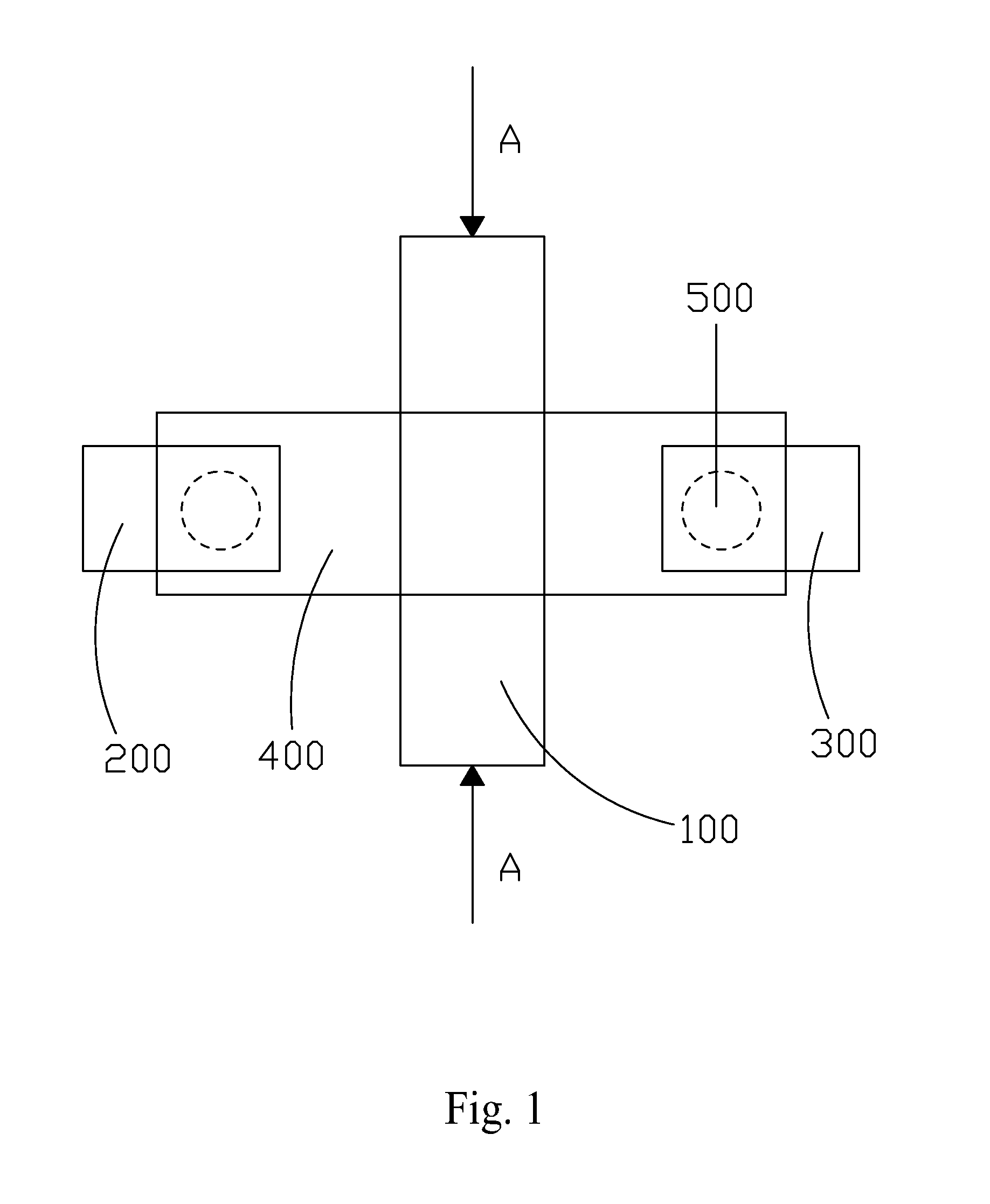
[0039]FIG. 1 is a schematic plan view showing a low temperature poly-silicon (LTPS) thin-film transistor (TFT). The LTPS TFT comprises a gate 100, a source 200, a drain 300, and an active layer 400. The source 200 and the drain 300 are respectively connected by vias 500 to the active layer 400.

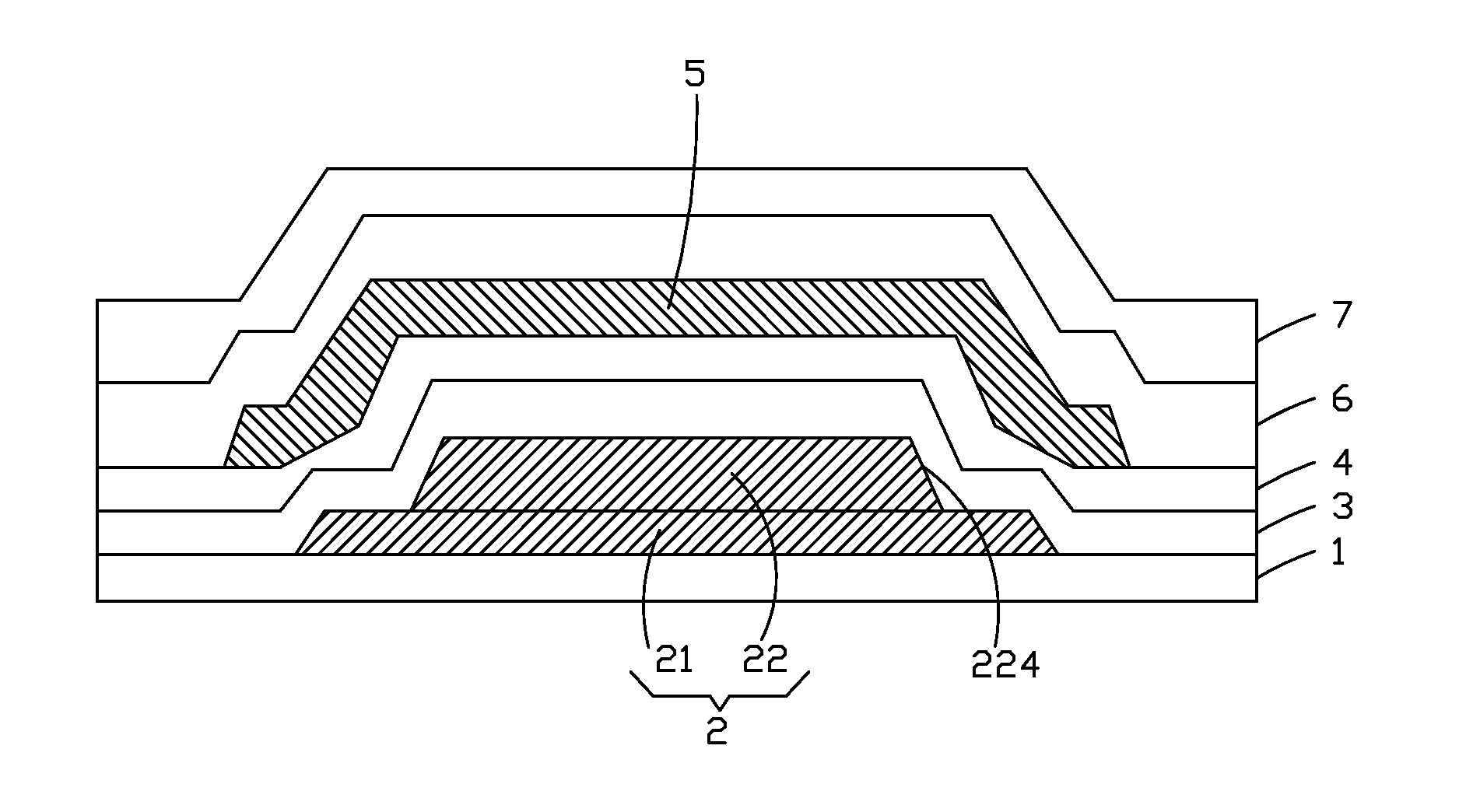
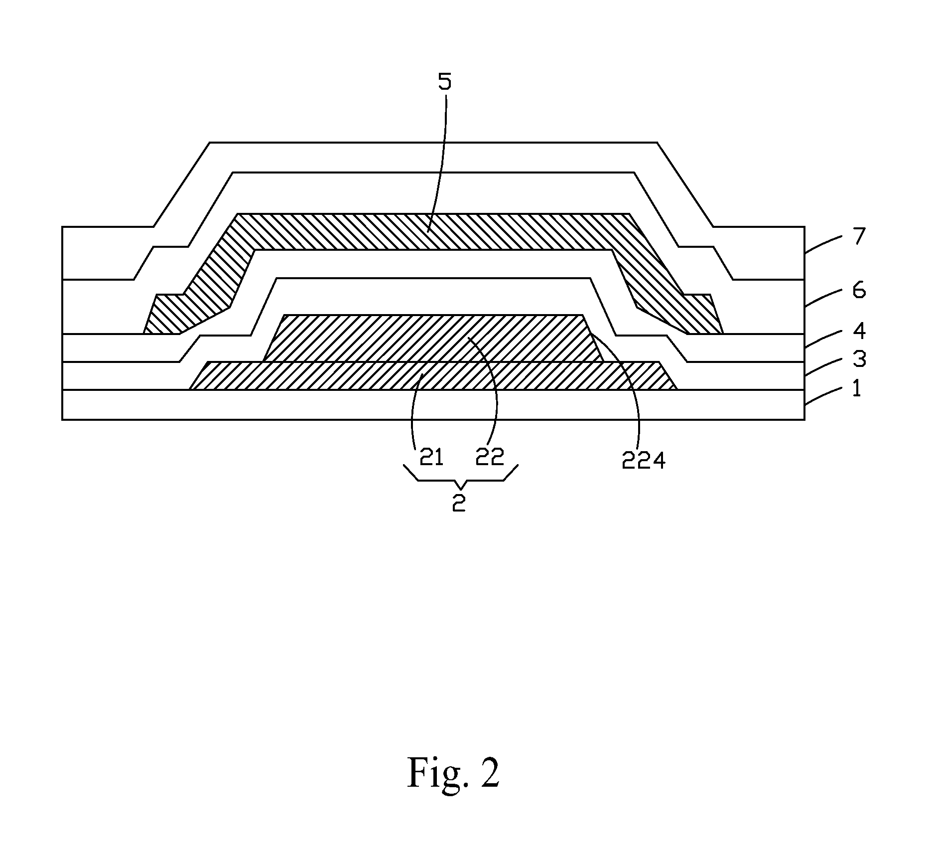
[0040]FIG. 2 is a cross-sectional view of the LTPS TFT according to the present invention taken along line A-A. As shown in FIG. 2, the present invention provides a LTPS TFT, which comprises: a substrate 1, a light shield layer 2 formed on the substrate 1, a pad layer 3 formed on the light shield layer 2, a dielectric layer 4 formed on the pad layer 3, an active layer 5 formed on the dielectric layer 4, a gate insulation layer 6 formed on the active layer 5, and a gate layer 7 fo...


PUM


Abstract

The present invention provides a low temperature poly-silicon thin-film transistor, as well as a manufacturing method thereof, which includes: a substrate (1), a light shield layer (2) formed on the substrate (1), a pad layer (3) formed on the light shield layer (2), a dielectric layer (4) formed on the pad layer, an active layer (5) formed on the dielectric layer, a gate insulation layer (6) formed on the active layer (5), and a gate layer (7) formed on the gate insulation layer (6). The light shield layer (2) includes a planar section (21) formed on the substrate (1) and a raised section (22) formed on the planar section (21). The active layer (5) has a projection that covers at least a partial area of an upper surface of the raised section (22) and one of sidewalls (224) of the raised section (22). Without varying an aperture ratio of a display device, the channel width can be effectively increased and the width-to-length ratio can be increased so as to increase an open state current and enhance driving power of the LTPS TFT and device performance.

Description

BACKGROUND OF THE INVENTION[0001]1. Field of the Invention[0002]The present invention relates to the field of displaying technology, and in particular to a low temperature poly-silicon thin-film transistor and a manufacturing method thereof.[0003]2. The Related Arts[0004]With the development of the displaying technology, flat panel displays, which have various advantages, such as high image quality, low power consumption, thin device body, and wide applications, have been widely used in various electronic consumer electronic products, such as mobile phones, televisions, personal digital assistants (PDAs), digital cameras, notebook computers, and desktop computers, and become the main stream of the display devices.[0005]Active matrix (AM) flat panel displays are one of the most commonly used display device today. The active matrix flat panel display device includes a thin-film transistor to control input of a data signal in order to the control the displaying of an image.[0006]Curren...

Claims


Application Information

Patent Timeline
IPC IPC(8): H01L29/786H01L21/306H01L27/32H01L21/02H01L29/06H01L29/66
CPCH01L29/78675H01L29/0684H01L29/66757H01L27/3272H01L2227/323H01L21/30604H01L21/02592H01L21/02532H01L21/02667H01L29/0607H01L29/6675H01L29/78672H01L29/78633H10K59/126H10K59/1201H01L29/786
Inventor LI, JINMING
Owner TCL CHINA STAR OPTOELECTRONICS TECH CO LTD
Why Eureka
Try Eureka