Organic light-emitting device and organic display device
a light-emitting device and organic technology, applied in semiconductor devices, photovoltaic energy generation, solid-state devices, etc., can solve the problems of easy degradation of the electron transport layer, and achieve the effects of high charge injection characteristics, high light emission efficiency, and high quality
- Summary
- Abstract
- Description
- Claims
- Application Information
AI Technical Summary
Benefits of technology
Problems solved by technology
Method used
Image
Examples
embodiment 1
[0057]1. Overall Configuration of Organic EL Display Device 1
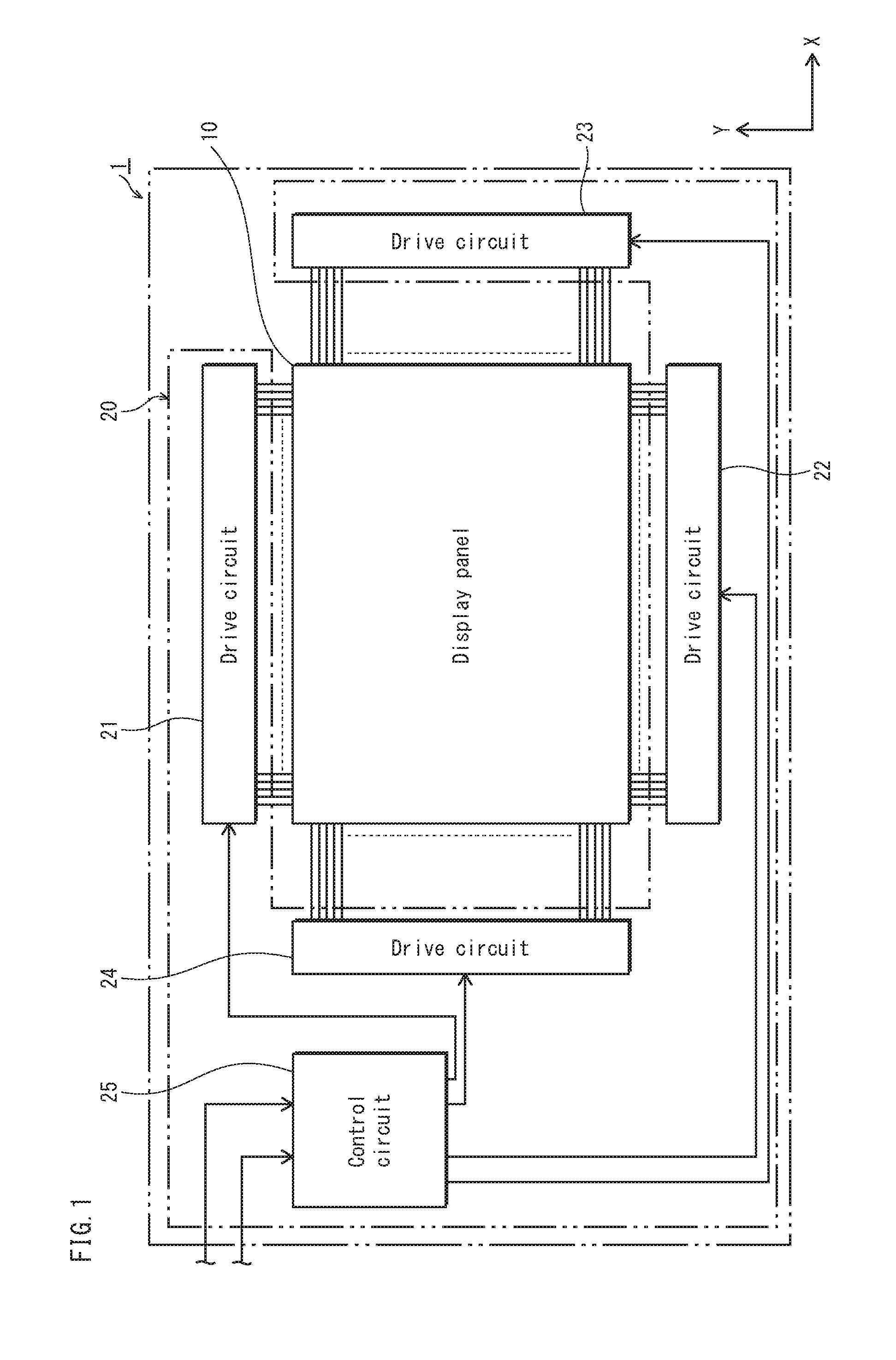
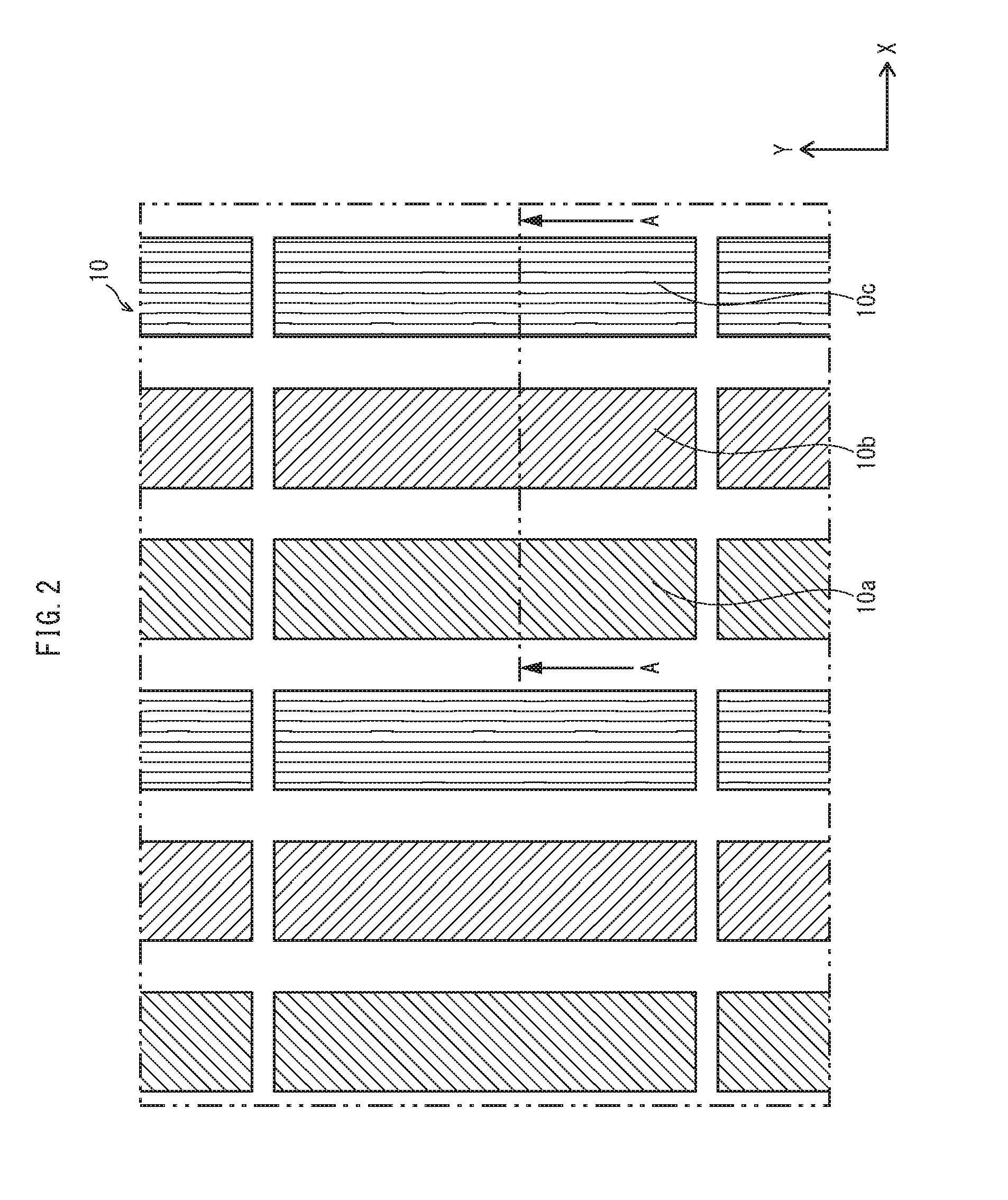
[0058]The overall configuration of an organic EL display device 1 pertaining to Embodiment 1 of the present invention is described with reference to FIGS. 1 and 2.
[0059]As illustrated in FIG. 1, the organic EL display device 1 includes a display panel 10 and a drive / control circuit unit 20 connected to the display panel 10. The display panel 10 is an organic EL panel employing the electroluminescence effect of organic material, and has a plurality of pixels.
[0060]As illustrated in FIG. 2, each pixel of the display panel 10 is made up of a sub-pixel 10a that is a light emitter of the color red (R), a sub-pixel 10b that is a light emitter of the color green (G), and a sub-pixel 10c that is a light emitter of the color blue (B). In the present Embodiment, the sub-pixels 10a, 10b, and 10c are arranged along the X axis and the Y axis to form a matrix (i.e., the sub-pixels are two-dimensionally disposed).
[0061]Returning to FIG. ...
implementation example
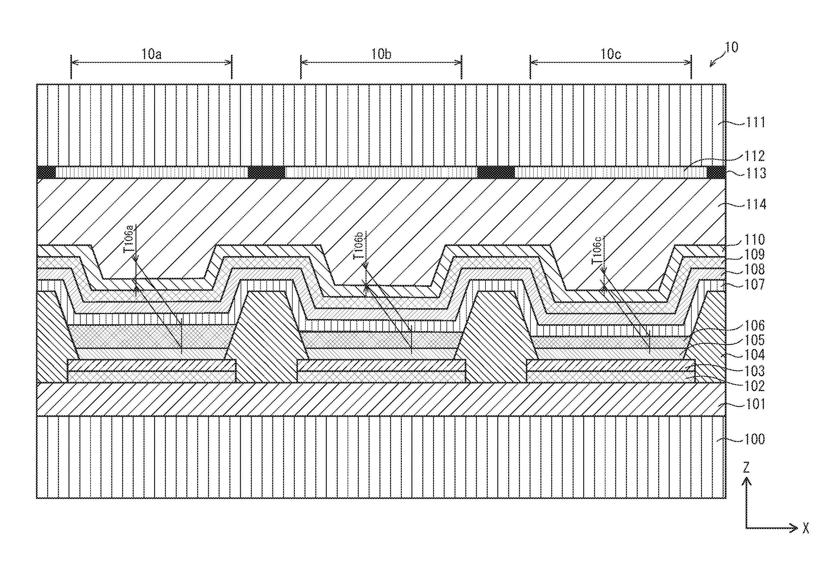
[0127]The display panel 10 pertaining to Embodiment 1, which has been described above and is illustrated in FIG. 3, etc., is used as an implementation example. Note that the measurement of surface shape was performed with respect to the sub-pixel 10a, in which the organic light-emitting layer 106 has the greatest thickness T106a, among the sub-pixels 10a through 10c.
[0128]Note that the X-direction size of the sub-pixel 10a is 65 μm and the Y-direction size of the sub-pixel 10a is 250 μm.
[0129]In addition, the first banks 104 and the second banks 115 are formed so that the heights H104 and H115 respectively illustrated in FIGS. 4B and 4C satisfied H115 / H104=54%.
[0130]Further, the first banks 104 are formed so that the lateral surface portions 104a of the first banks 104 have a contact angle between 45° and 60° (with respect to anisole), and the second banks 115 are formed so that the lateral surface portions 115a of the second banks 115 have a contact angle of 5° of smaller (with re...
implementation example 1
[0152]Implementation example 1 is a display panel having the same structure as the display panel 1. In implementation example 1, the width W2B of each second bank 115 is 70 μm. Further, in implementation example 1, the sub-pixels 10a, 10b, and 10c have the same size as in the above, i.e., 65 μm×250 μm. As such, in the implementation example 1, the ratio of the width W2B to the longitudinal-direction size of the sub-pixels 10a, 10b, and 10c is approximately 28%.
PUM
 Abstract
Description
Claims
Application Information


