
Fingerprint recogntion sensor and terminal device

a terminal device and fingerprint recognition technology, applied in the field of fingerprint identification, can solve the problems of limiting the application scope of fingerprint identification sensors, affecting the accuracy of fingerprint recognition, so as to achieve greater capacitance, higher voltage, and strong coupling

Active Publication Date: 2016-12-15
SHENZHEN GOODIX TECH CO LTD
View PDF2 Cites 14 Cited by
  • Summary
  • Abstract
  • Description
  • Claims
  • Application Information

AI Technical Summary

Benefits of technology

This patent is about a new fingerprint identification sensor for terminal devices. The sensor doesn't need a metal ring, so it can be used on devices like phones and tablets without having to create a hole in the surface. This expands the scope of who can use the sensor. Additionally, the sensor uses capacitance to create a clear fingerprint image and has improved fingerprint identification compared to other sensors.

Problems solved by technology

However, in some application scenarios, for example, the appearance design of a mobile phone and a tablet personal computer, to achieve mirror-like screen effect and improve water proof performance, it is not suitable to open a hole on the screen, which restricts the application scope of the fingerprint identification sensor.
When the terminal device is provided with a metal housing, and the device is held in one user's hand, the attenuation to the driving signal will be more serious, thereby reducing clarity of the fingerprint image, and affecting the fingerprint identification effect.

Method used


Image

  • Fingerprint recogntion sensor and terminal device
  • Fingerprint recogntion sensor and terminal device
  • Fingerprint recogntion sensor and terminal device

Examples


first embodiment

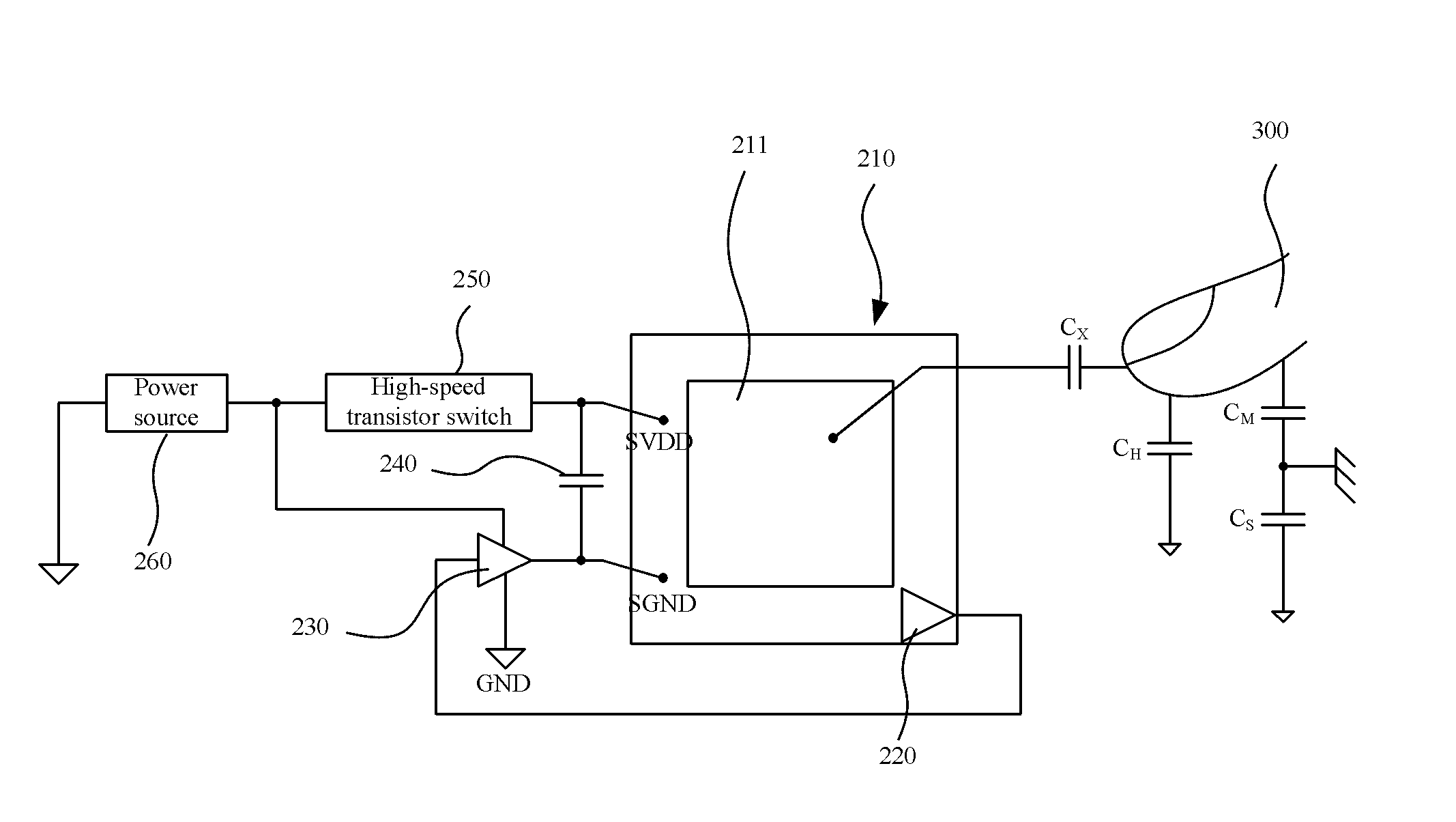
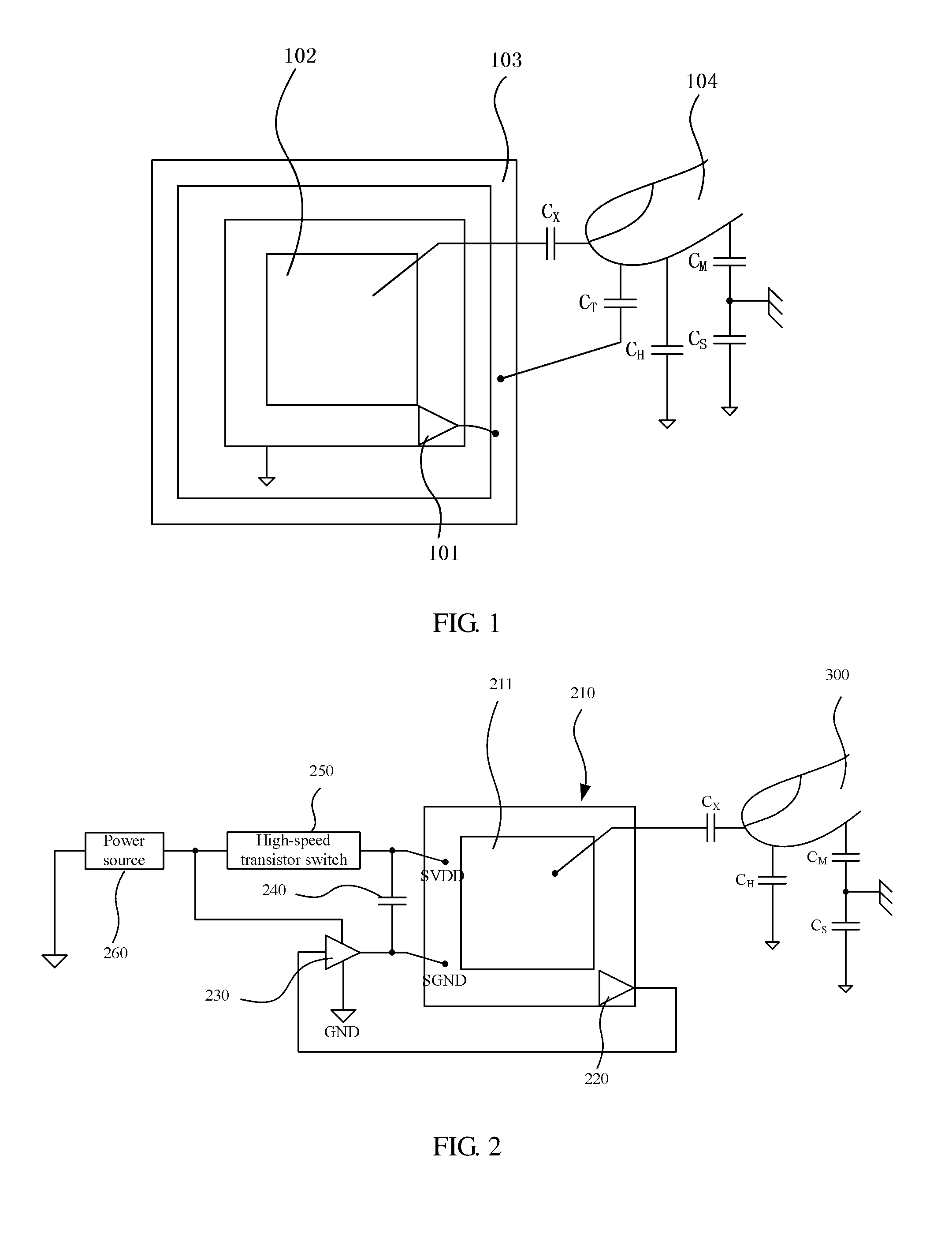
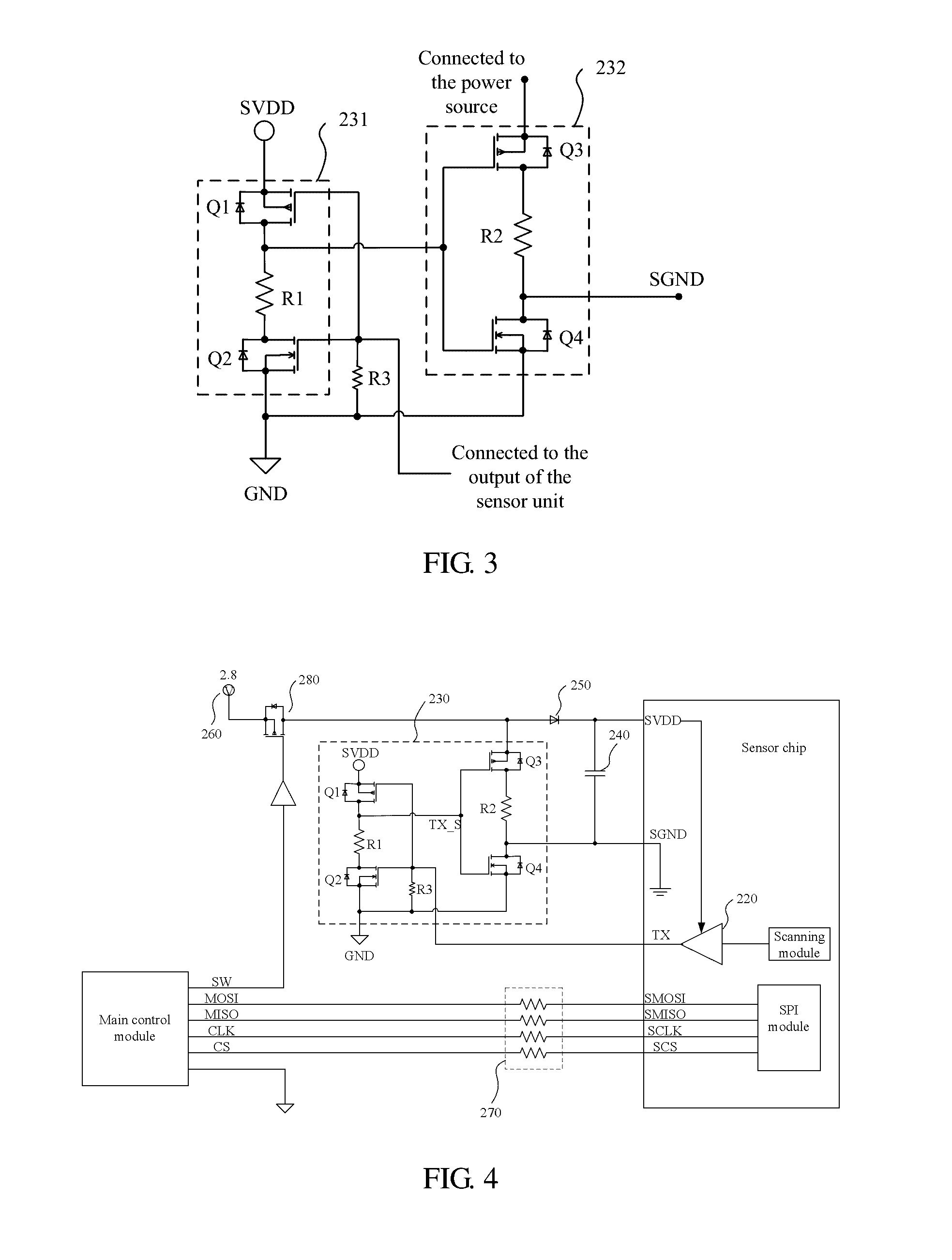
[0055]FIG. 4 illustrates specific application of the fingerprint identification sensor according to the present invention. In this embodiment, the sensor unit is integrated in a sensor chip, wherein the sensor chip comprises a scanning module and a serial peripheral interface (SPI) module. The scanning module outputs a driving signal to scan the capacitor array. The SPI module provides an SPI interface which acts as a communication interface of the sensor chip which is connected to a communication interface of a main control module of the terminal device, in order to communicate with the main control module via the communication interface of the main control module. For example, the sensor chip sends fingerprint image data to the main control module, and the main control module sends a control command or the like to the sensor chip. The communication interface may be an inter-integrated circuit (I2C) interface, a serial / parallel interface or the like, in addition to the SPI interfac...

fourth embodiment

[0073]FIG. 8 illustrates the fingerprint identification sensor according to the present invention. In this embodiment, the sensor unit and the relay module are integrated in a sensor chip. In this way, the size of a fingerprint identification system is further reduced, to accommodate to the demand on a small-size terminal device.

[0074]The fingerprint identification sensor according to the embodiment of the present invention is capable of operating without a driving metal ring. Therefore, there is no need to open a hole in the surface of the terminal device, and the sensor only needs to be installed in a specific zone under an insulation plate of the device, which implements the invisible fingerprint sensor (IFS) technology. FIG. 9 illustrates an application scenario where the IFS technology is applied to a smart phone. The smart phone comprises a display screen cover plate 10, wherein a screen display region 20 is located at a central region of the screen, and a fingerprint identifi...


PUM


Abstract

Disclosed is a fingerprint identification sensor, which comprises: a sensor unit, comprising a capacitor array formed by a plurality of capacitor induction units and having an output, a power supply and a sensor ground output; a conversion circuit, connected to the device ground of the terminal device, and the output and the sensor ground of the sensor unit, and configured to, upon modulating the driving signal to the modulated signal, output the modulated signal to the sensor ground; an energy storage capacitor, connected between the power supply and the sensor ground, and configured to stabilize an operating voltage of the sensor unit; a high-speed transistor switch, connected to the power supply, and configured to perform synchronous switch-on and switch-off according to status of the conversion circuit power supply; and a power supply, connected to the conversion circuit and the power supply of the sensor unit via the high-speed transistor switch.

Description

CROSS-REFERENCE TO RELATED APPLICATIONS[0001]This application is a continuation of International Patent Application No. PCT / CN2015 / 072430, with an international filing date of Feb. 6, 2015, designating the United States, now pending, which is based on Chinese Patent Application No. 201410849191.9, filed Dec. 30, 2014. The contents of these specifications are incorporated herein by reference.BACKGROUND OF THE INVENTION[0002]Field of the Invention[0003]The present invention relates to the technical field of fingerprint identification, and in particular, relates to a fingerprint identification sensor and a terminal device.[0004]Description of the Related Art[0005]The fingerprint identification technology is widely applied in the field of the electronic security, and is a reliable method for implementing identity authentication. A capacitive fingerprint identification sensor is one of the widely used fingerprint sensors, and is formed by a miniaturized capacitor polar plate array. An up...

Claims


Application Information

Patent Timeline
Patent Type & Authority Applications(United States)
IPC IPC(8): G06K9/00
CPCG06K9/0002G06V40/1306H03K17/962
Inventor DU, CANHONGZHUO, GUANGMING
Owner SHENZHEN GOODIX TECH CO LTD
Learn More