Substrate processing method and substrate processing apparatus

a substrate processing and substrate technology, applied in the manufacture of microstructural devices, microstructures, electrical devices, etc., can solve the problems of defects in drying, inability to remove the rinsing liquid,

Active Publication Date: 2016-12-15
DAINIPPON SCREEN MTG CO LTD
View PDF9 Cites 2 Cited by
  • Summary
  • Abstract
  • Description
  • Claims
  • Application Information

AI Technical Summary

Benefits of technology

[0039]According to this arrangement, it is possible to keep the internal space in a closed state by closing the exhaust unit that exhausts the internal space of the seal chamber. This makes it possible to reliably form a thin film of an organic solvent that has a uniform, small thickn

Problems solved by technology

If a fine pattern is formed on the front surface of the substrate, there is a fear that it will be impossible to remove the rinsing l

Method used


Image

  • Substrate processing method and substrate processing apparatus
  • Substrate processing method and substrate processing apparatus
  • Substrate processing method and substrate processing apparatus

Examples


Embodiment Construction

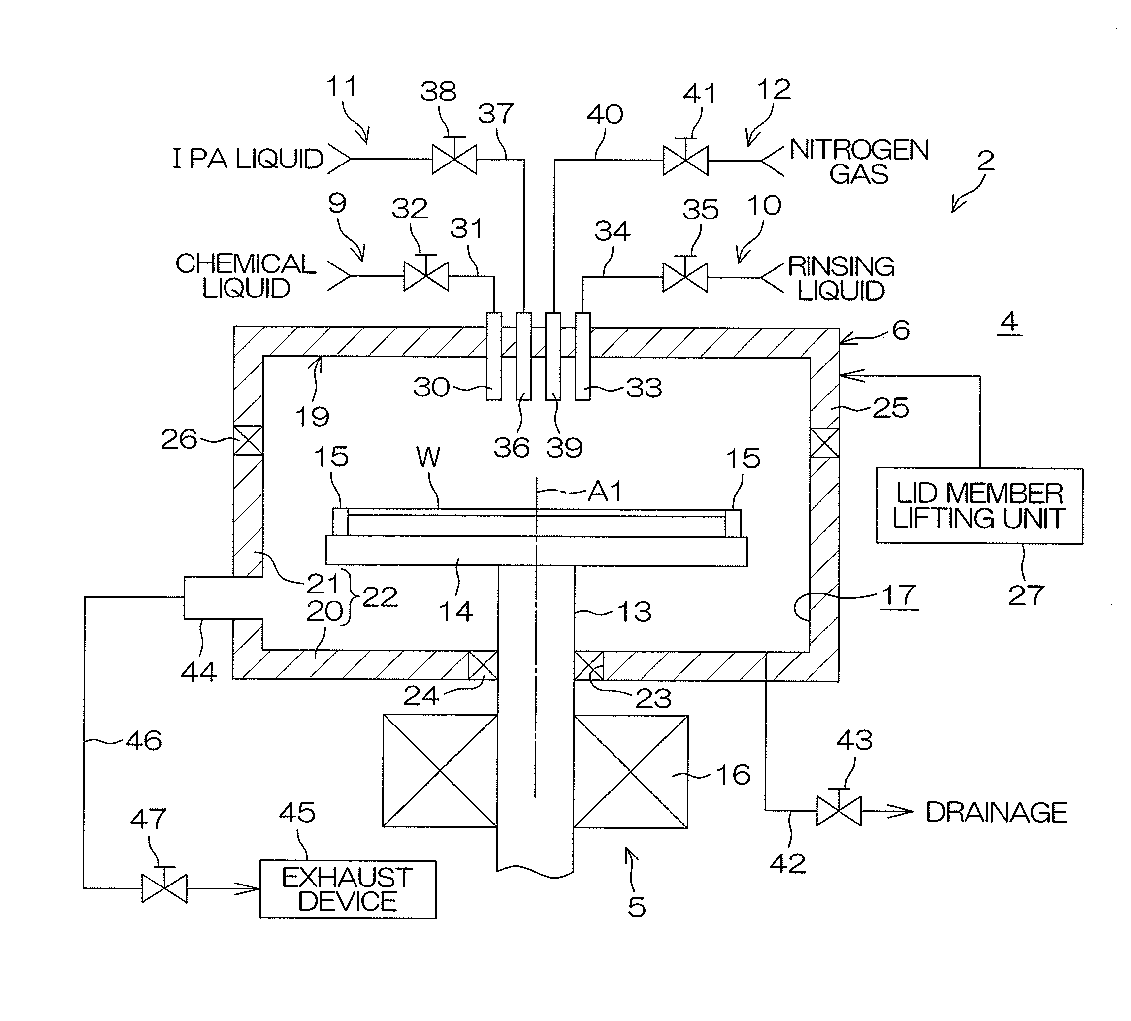
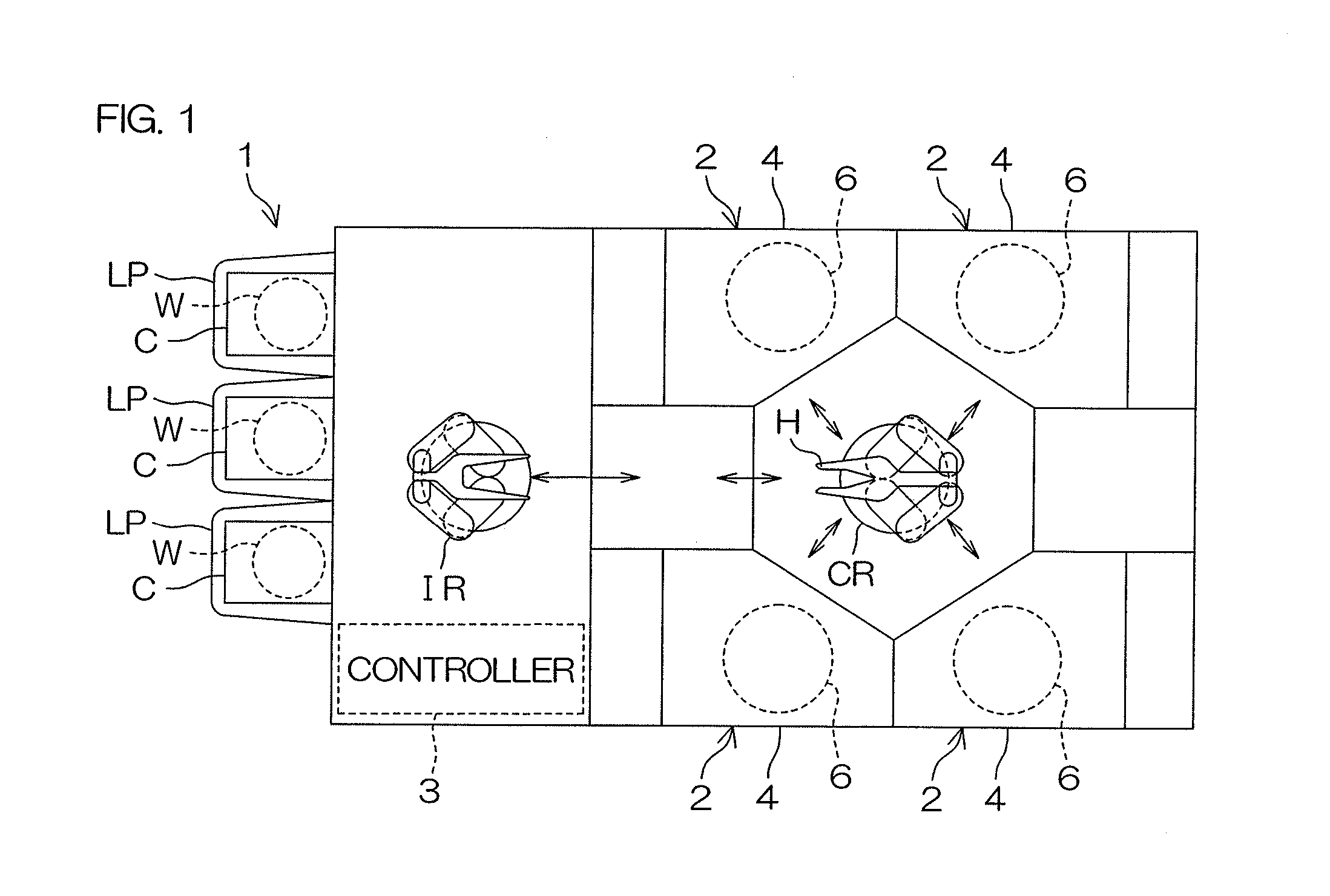
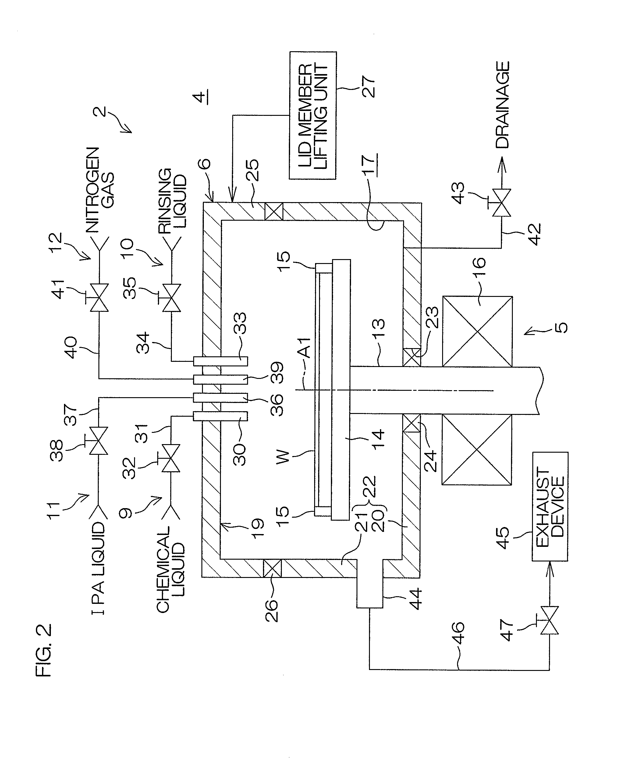
[0050]FIG. 1 is a plan view schematically to describe the layout of the inside of a substrate processing apparatus according to a first preferred embodiment of the present invention. The substrate processing apparatus 1 is a single substrate processing type apparatus that processes substrates W, such as silicon wafers, one by one. In this preferred embodiment, the substrate W is a disk-shaped substrate. The substrate processing apparatus 1 includes a plurality of processing units 2 each of which processes a substrate W by use of a processing liquid, a load port LP on which a carrier C that contains a plurality of substrates W to be processed by the processing unit 2 is placed, transfer robots IR and CR that convey substrates W between the load port LP and the processing unit 2, and a controller 3 that controls the substrate processing apparatus 1. The transfer robot IR conveys substrates W between the carrier C and the transfer robot CR. The transfer robot CR conveys substrates W be...


PUM


Abstract

A substrate processing method includes a liquid film forming step of forming a liquid film of an organic solvent with which a whole area of an upper surface of a substrate is covered in order to replace a processing liquid existing on the upper surface with an organic solvent liquid, a thin film holding step of thinning the liquid film of the organic solvent by rotating the substrate at a first high rotational speed while keeping surroundings of the whole area of the upper surface in an atmosphere of an organic solvent vapor and holding a resulting thin film of the organic solvent on the upper surface, and a thin-film removing step of removing the thin film from the upper surface after the thin film holding step, and the thin-film removing step includes a high-speed rotation step of rotating the substrate at a second high rotational speed.

Description

BACKGROUND OF THE INVENTION[0001]1. Field of the Invention[0002]The present invention relates to a substrate processing method and a substrate processing apparatus for processing substrates. Examples of substrates to be processed include semiconductor wafers, substrates for liquid crystal displays, substrates for plasma displays, substrates for FEDs (Field Emission Displays), substrates for optical disks, substrates for magnetic disks, substrates for magneto-optical disks, substrates for photomasks, ceramic substrates, and substrates for solar cells.[0003]2. Description of Related Art[0004]In steps of manufacturing a semiconductor device, a front surface of a substrate, such as a semiconductor wafer, is processed by a processing liquid. A single substrate processing type apparatus that processes substrates one by one includes a spin chuck that rotates a substrate while holding the substrate substantially horizontally and a nozzle that supplies a processing liquid to the front surfac...

Claims


Application Information

Patent Timeline
IPC IPC(8): H01L21/02H01L21/67H01L21/306
CPCH01L21/0206H01L21/6704H01L21/30604H01L21/02057H01L21/67023H01L21/67028H01L21/67051H01L21/02052H01L21/02307H01L21/02343H01L21/67017H01L21/67126H01L21/6715H01L21/68764B81C1/00928H01L21/02063
Inventor IWAHATA, SHOTAOTSUJI, MASAYUKI
Owner DAINIPPON SCREEN MTG CO LTD
Why Eureka
Try Eureka