Method and apparatus for controlled dopant incorporation and activation in a chemical vapor deposition system

a technology of chemical vapor deposition system and controlled dopant, which is applied in the direction of chemical vapor deposition coating, coating, semiconductor devices, etc., can solve the problems of inefficiency of post-growth annealing procedures, reduced overall electrically active dopant levels, and passivation or compensation of mg acceptor levels, so as to reduce the quantity of point defects

a technology of chemical vapor deposition system and controlled dopant, which is applied in the direction of chemical vapor deposition coating, coating, semiconductor devices, etc., can solve the problems of inefficiency of post-growth annealing procedures, reduced overall electrically active dopant levels, and passivation or compensation of mg acceptor levels, so as to reduce the quantity of point defects

US20170032974A1Inactive Publication Date: 2017-02-02VEECO INSTR

Image

  • Method and apparatus for controlled dopant incorporation and activation in a chemical vapor deposition system
  • Method and apparatus for controlled dopant incorporation and activation in a chemical vapor deposition system
  • Method and apparatus for controlled dopant incorporation and activation in a chemical vapor deposition system

Examples


Embodiment Construction

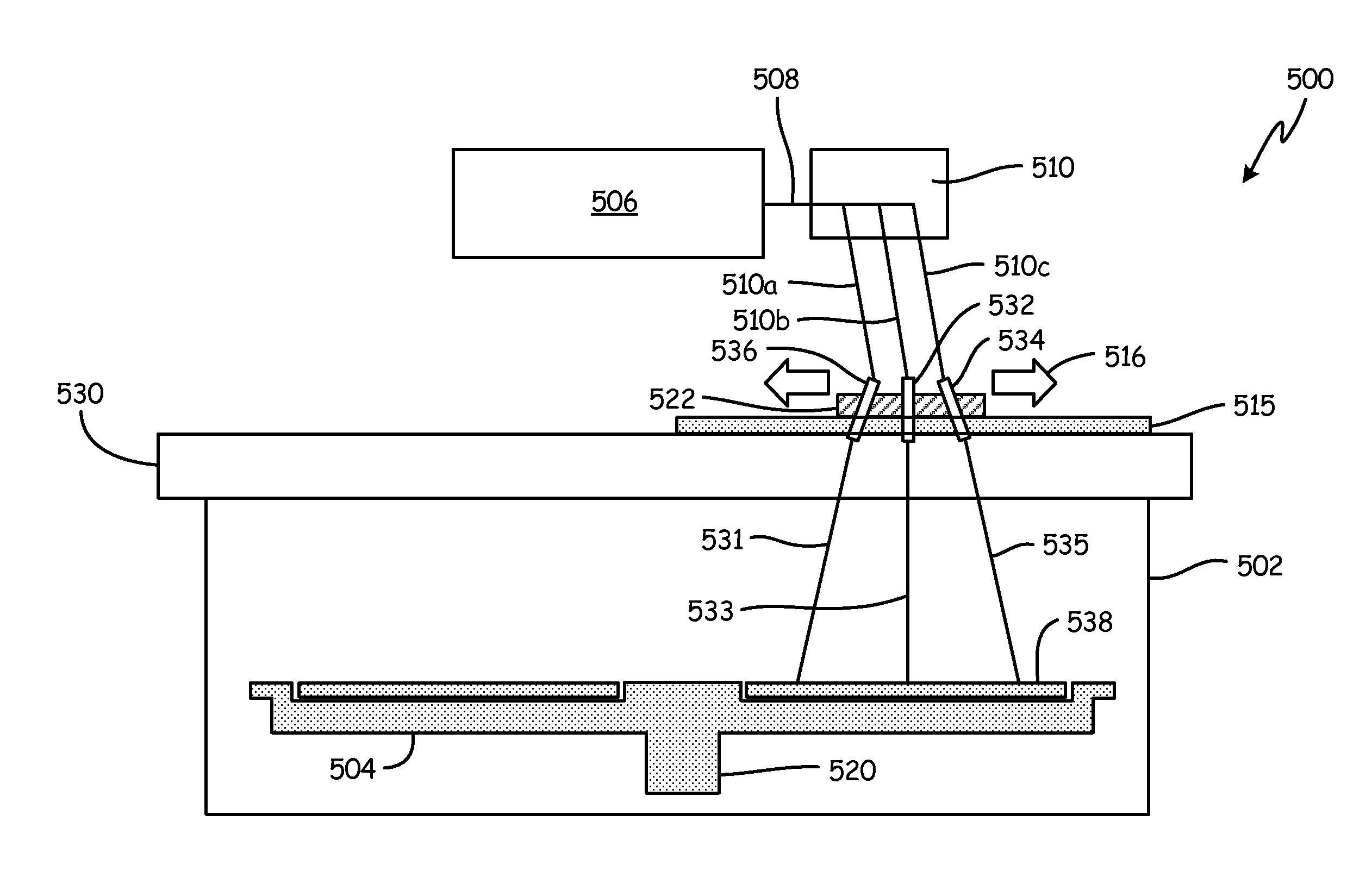
[0021]According to embodiments, a Metal Organic Chemical Vapor Deposition (MOCVD) system includes a chemical vapor deposition reactor having a window through which ultraviolet (UV) light can be routed. The UV light can be provided by a UV light source that is both tunable to different wavelengths, as well as capable of being aimed at specific portions of the interior of a chamber of the MOCVD system. For example, the UV light could be a mercury arc lamp, a mercury-xenon arc lamp, or a UV LED or LED array. In various embodiments, the UV lights are adapted to be tuned to a desired wavelength in the UV spectrum (typically about 180 nm to about 400 nm), and to be used to generate a beam of light that can be aimed at various parts of the semiconductor layer being grown in the MOCVD chamber in a raster pattern. The raster speed (defining the dwell time per illuminated area), UV light wavelength, and light intensity can each be modified to modulate the growth characteristics of the semicon...


PUM

PropertyMeasurementUnit
wavelengthaaaaaaaaaa
pressureaaaaaaaaaa
pressureaaaaaaaaaa

Abstract

Embodiments include systems and methods for producing semiconductor wafers having reduced quantities of point defects. These systems and methods include a tunable ultraviolet (UV) light source, which is controlled to produce a raster of a UV light beam across a surface of a semiconductor wafer during epitaxial growth to dissociate point defects in the semiconductor wafer. In various embodiments, the tunable UV light source is configured external to a Metal Organic Chemical Vapor Deposition (MOCVD) chamber and controlled such that the UV light beam is directed though a window defined in a wall of the MOCVD chamber.

Description

TECHNICAL FIELD[0001]Embodiments relate to processes or apparatuses specially adapted for the manufacture or treatment of semiconductor or solid-state devices or of parts thereof. More specifically, embodiments relate to using reduction or decomposition of a gaseous compound yielding a solid condensate (i.e., chemical vapor deposition or Metal Organic Chemical Vapor Deposition (MOCVD)), and bombardment of such structures with optical radiation during manufacture.BACKGROUND[0002]Chemical vapor deposition involves directing one or more gases containing chemical species onto a surface of a substrate so that the reactive species react and form a deposit on the surface. For example, compound semiconductors can be formed by epitaxial growth of a semiconductor material on a substrate. The substrate typically is a crystalline material in the form of a disc, commonly referred to as a “wafer.” Compound semiconductors such as III-V semiconductors commonly are formed by growing layers of the co...

Claims


Application Information

Patent Timeline
02 Feb 2017
Publication
US20170032974A1
IPC
H01L21/324; H01L29/20; H01L29/205; H01L29/778; C23C16/04; H01L33/32; H01L33/00; C23C16/48; C23C16/52; C23C16/458; H01L21/02; H01L29/66
CPC
H01L21/3245; H01L21/0262; H01L29/20; H01L29/205; H01L29/2003; H01L29/7787; C23C16/047; H01L33/32
Inventors
ARMOUR, ERIC; PAPASOULIOTIS, GEORGE